- 您现在的位置:买卖IC网 > PDF目录13888 > LT3680EMSE#TRPBF (Linear Technology)IC REG BUCK ADJ 3.5A 10MSOP PDF资料下载
参数资料
| 型号: | LT3680EMSE#TRPBF |
| 厂商: | Linear Technology |
| 文件页数: | 14/24页 |
| 文件大小: | 0K |
| 描述: | IC REG BUCK ADJ 3.5A 10MSOP |
| 标准包装: | 2,500 |
| 类型: | 降压(降压) |
| 输出类型: | 可调式 |
| 输出数: | 1 |
| 输出电压: | 0.79 V ~ 30 V |
| 输入电压: | 3.6 V ~ 36 V |
| PWM 型: | 电流模式,混合 |
| 频率 - 开关: | 230kHz ~ 2.45MHz |
| 电流 - 输出: | 3.5A |
| 同步整流器: | 无 |
| 工作温度: | -40°C ~ 125°C |
| 安装类型: | 表面贴装 |
| 封装/外壳: | 10-TFSOP,10-MSOP(0.118",3.00mm 宽)裸露焊盘 |
| 包装: | 带卷 (TR) |
| 供应商设备封装: | 10-MSOP 裸露焊盘 |
�� �
�
�LT3680�
�APPLICATIONS� INFORMATION�
�Low-Ripple� Burst� Mode� and� Pulse-Skip� Mode�
�The� LT3680� is� capable� of� operating� in� either� Low-Ripple� Burst�
�Mode� or� pulse-skipping� mode� which� are� selected� using� the�
�SYNC� pin.� See� the� Synchronization� section� for� details.�
�To� enhance� ef?ciency� at� light� loads,� the� LT3680� can� be�
�operated� in� Low-Ripple� Burst� Mode� operation� which� keeps�
�the� output� capacitor� charged� to� the� proper� voltage� while�
�minimizing� the� input� quiescent� current.� During� Burst� Mode�
�operation,� the� LT3680� delivers� single� cycle� bursts� of� current�
�to� the� output� capacitor� followed� by� sleep� periods� where�
�the� output� power� is� delivered� to� the� load� by� the� output�
�capacitor.� Because� the� LT3680� delivers� power� to� the� output�
�with� single,� low� current� pulses,� the� output� ripple� is� kept�
�below� 15mV� for� a� typical� application.� In� addition,� V� IN� and�
�BD� quiescent� currents� are� reduced� to� typically� 30μA� and�
�90μA� respectively� during� the� sleep� time.� As� the� load� current�
�decreases� towards� a� no� load� condition,� the� percentage� of�
�time� that� the� LT3680� operates� in� sleep� mode� increases�
�and� the� average� input� current� is� greatly� reduced� resulting�
�in� high� ef?ciency� even� at� very� low� loads.� See� Figure� 4.�
�At� higher� output� loads� (above� 140mA� for� the� front� page�
�application)� the� LT3680� will� be� running� at� the� frequency�
�programmed� by� the� R� T� resistor,� and� will� be� operating� in�
�standard� PWM� mode.� The� transition� between� PWM� and�
�Low-Ripple� Burst� Mode� is� seamless,� and� will� not� disturb�
�the� output� voltage.�
�If� low� quiescent� current� is� not� required� the� LT3680� can�
�operate� in� Pulse-Skip� mode.� The� bene?t� of� this� mode� is�
�that� the� LT3680� will� enter� full� frequency� standard� PWM�
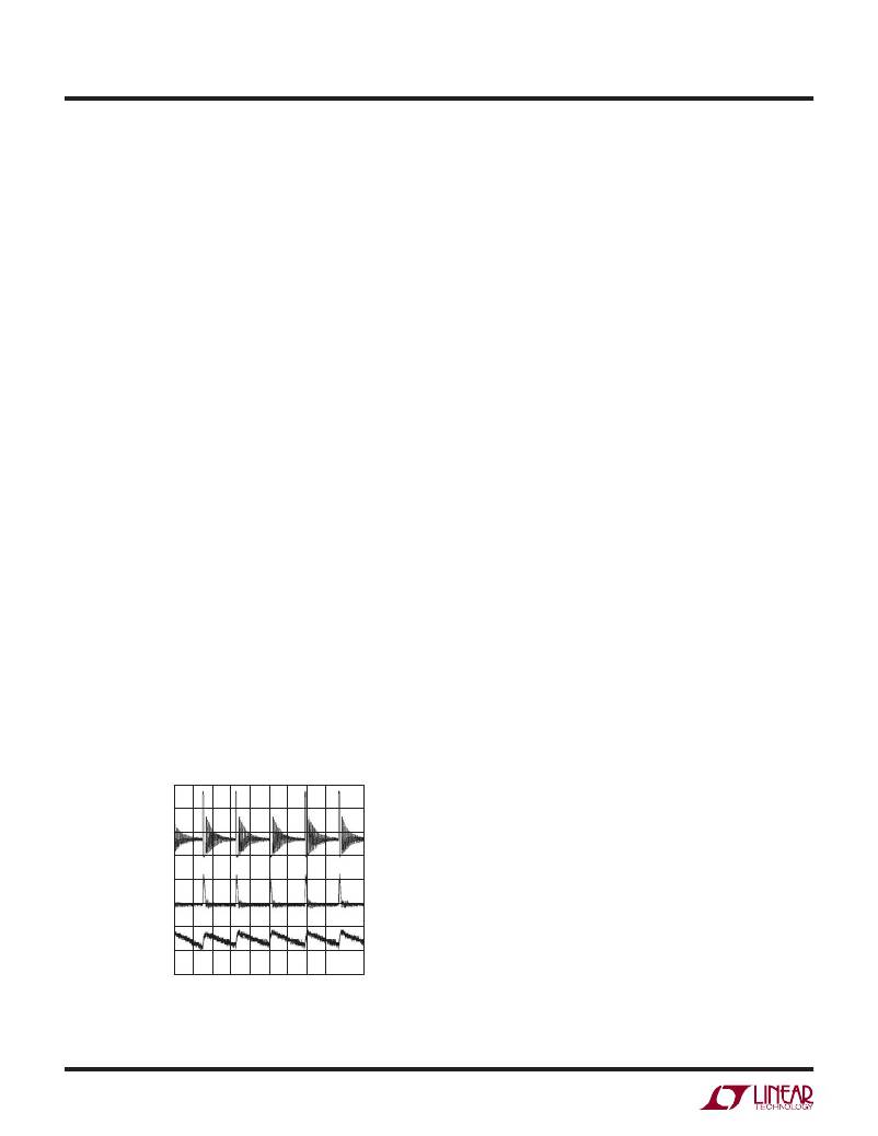
�V� SW�
�5V/DIV�
�I� L�
�0.2A/DIV�
�V� OUT�
�10mV/DIV�
�operation� at� a� lower� output� load� current� than� when� in� Burst�
�Mode.� The� front� page� application� circuit� will� switch� at� full�
�frequency� at� output� loads� higher� than� about� 60mA.� Select�
�pulse-skipping� mode� by� applying� a� clock� signal� or� a� DC�
�voltage� higher� than� 0.8V� to� the� SYNC� pin.�
�BOOST� and� BIAS� Pin� Considerations�
�Capacitor� C3� and� the� internal� boost� Schottky� diode� (see�
�the� Block� Diagram)� are� used� to� generate� a� boost� volt-�
�age� that� is� higher� than� the� input� voltage.� In� most� cases�
�a� 0.22μF� capacitor� will� work� well.� Figure� 2� shows� three�
�ways� to� arrange� the� boost� circuit.� The� BOOST� pin� must� be�
�more� than� 2.3V� above� the� SW� pin� for� best� ef?ciency.� For�
�outputs� of� 3V� and� above,� the� standard� circuit� (Figure� 5a)�
�is� best.� For� outputs� between� 2.8V� and� 3V,� use� a� 1μF� boost�
�capacitor.� A� 2.5V� output� presents� a� special� case� because� it�
�is� marginally� adequate� to� support� the� boosted� drive� stage�
�while� using� the� internal� boost� diode.� For� reliable� BOOST� pin�
�operation� with� 2.5V� outputs� use� a� good� external� Schottky�
�diode� (such� as� the� ON� Semi� MBR0540),� and� a� 1μF� boost�
�capacitor� (see� Figure� 5b).� For� lower� output� voltages� the�
�boost� diode� can� be� tied� to� the� input� (Figure� 5c),� or� to�
�another� supply� greater� than� 2.8V.� Tying� BD� to� V� IN� reduces�
�the� maximum� input� voltage� to� 28V.� The� circuit� in� Figure� 5a�
�is� more� ef?cient� because� the� BOOST� pin� current� and� BD�
�pin� quiescent� current� comes� from� a� lower� voltage� source.�
�You� must� also� be� sure� that� the� maximum� voltage� ratings�
�of� the� BOOST� and� BD� pins� are� not� exceeded.�
�The� minimum� operating� voltage� of� an� LT3680� application�
�is� limited� by� the� minimum� input� voltage� (3.6V)� and� by� the�
�maximum� duty� cycle� as� outlined� in� a� previous� section.� For�
�proper� startup,� the� minimum� input� voltage� is� also� limited�
�by� the� boost� circuit.� If� the� input� voltage� is� ramped� slowly,�
�or� the� LT3680� is� turned� on� with� its� RUN/SS� pin� when� the�
�output� is� already� in� regulation,� then� the� boost� capacitor�
�may� not� be� fully� charged.� Because� the� boost� capacitor� is�
�charged� with� the� energy� stored� in� the� inductor,� the� circuit�
�will� rely� on� some� minimum� load� current� to� get� the� boost�
�circuit� running� properly.� This� minimum� load� will� depend�
�on� input� and� output� voltages,� and� on� the� arrangement� of�
�V� IN� =� 12V�
�5μs/DIV�
�3680� F04�
�the� boost� circuit.� The� minimum� load� generally� goes� to�
�V� OUT� =� 3.3V�
�I� LOAD� =� 10mA�
�Figure� 4.� Burst� Mode� Operation�
�zero� once� the� circuit� has� started.� Figure� 6� shows� a� plot�
�of� minimum� load� to� start� and� to� run� as� a� function� of� input�
�voltage.� In� many� cases� the� discharged� output� capacitor�
�3680fb�
�14�
�相关PDF资料 |
PDF描述 |
|---|---|
| LT1534IS-1 | IC REG BOOST ADJ 2A 16SOIC |
| MAX6724AUTZED1+T | IC SUPERVISOR MPU SOT23-6 |
| LT1372HVIS8#TRPBF | IC REG MULTI CONFIG ADJ 8SOIC |
| MAX6724AUTZWD1+T | IC SUPERVISOR MPU SOT23-6 |
| LT1372HVIS8#TR | IC REG MULTI CONFIG ADJ 8SOIC |
相关代理商/技术参数 |
参数描述 |
|---|---|
| LT3680HMSE#PBF | 功能描述:IC REG BUCK ADJ 3.5A 10MSOP RoHS:是 类别:集成电路 (IC) >> PMIC - 稳压器 - DC DC 开关稳压器 系列:- 设计资源:Design Support Tool 标准包装:1 系列:- 类型:升压(升压) 输出类型:固定 输出数:1 输出电压:3V 输入电压:0.75 V ~ 2 V PWM 型:- 频率 - 开关:- 电流 - 输出:100mA 同步整流器:是 工作温度:-40°C ~ 85°C 安装类型:表面贴装 封装/外壳:SOT-23-5 细型,TSOT-23-5 包装:剪切带 (CT) 供应商设备封装:TSOT-23-5 其它名称:AS1323-BTTT-30CT |
| LT3680HMSE#TRPBF | 功能描述:IC REG BUCK ADJ 3.5A 10MSOP RoHS:是 类别:集成电路 (IC) >> PMIC - 稳压器 - DC DC 开关稳压器 系列:- 设计资源:Design Support Tool 标准包装:1 系列:- 类型:升压(升压) 输出类型:固定 输出数:1 输出电压:3V 输入电压:0.75 V ~ 2 V PWM 型:- 频率 - 开关:- 电流 - 输出:100mA 同步整流器:是 工作温度:-40°C ~ 85°C 安装类型:表面贴装 封装/外壳:SOT-23-5 细型,TSOT-23-5 包装:剪切带 (CT) 供应商设备封装:TSOT-23-5 其它名称:AS1323-BTTT-30CT |
| LT3680IDD#PBF | 功能描述:IC REG BUCK ADJ 3.5A 10DFN RoHS:是 类别:集成电路 (IC) >> PMIC - 稳压器 - DC DC 开关稳压器 系列:- 标准包装:250 系列:- 类型:降压(降压) 输出类型:固定 输出数:1 输出电压:1.2V 输入电压:2.05 V ~ 6 V PWM 型:电压模式 频率 - 开关:2MHz 电流 - 输出:500mA 同步整流器:是 工作温度:-40°C ~ 85°C 安装类型:表面贴装 封装/外壳:6-UFDFN 包装:带卷 (TR) 供应商设备封装:6-SON(1.45x1) 产品目录页面:1032 (CN2011-ZH PDF) 其它名称:296-25628-2 |
| LT3680IDD#TRPBF | 功能描述:IC REG BUCK ADJ 3.5A 10DFN RoHS:是 类别:集成电路 (IC) >> PMIC - 稳压器 - DC DC 开关稳压器 系列:- 设计资源:Design Support Tool 标准包装:1 系列:- 类型:升压(升压) 输出类型:固定 输出数:1 输出电压:3V 输入电压:0.75 V ~ 2 V PWM 型:- 频率 - 开关:- 电流 - 输出:100mA 同步整流器:是 工作温度:-40°C ~ 85°C 安装类型:表面贴装 封装/外壳:SOT-23-5 细型,TSOT-23-5 包装:剪切带 (CT) 供应商设备封装:TSOT-23-5 其它名称:AS1323-BTTT-30CT |
| LT3680IDDPBF | 制造商:Linear Technology 功能描述:36V 3.5A 2.4MHz Regulator 75uA DFN10EP |
发布紧急采购,3分钟左右您将得到回复。