- 您现在的位置:买卖IC网 > PDF目录13888 > LT3680EMSE#TRPBF (Linear Technology)IC REG BUCK ADJ 3.5A 10MSOP PDF资料下载
参数资料
| 型号: | LT3680EMSE#TRPBF |
| 厂商: | Linear Technology |
| 文件页数: | 16/24页 |
| 文件大小: | 0K |
| 描述: | IC REG BUCK ADJ 3.5A 10MSOP |
| 标准包装: | 2,500 |
| 类型: | 降压(降压) |
| 输出类型: | 可调式 |
| 输出数: | 1 |
| 输出电压: | 0.79 V ~ 30 V |
| 输入电压: | 3.6 V ~ 36 V |
| PWM 型: | 电流模式,混合 |
| 频率 - 开关: | 230kHz ~ 2.45MHz |
| 电流 - 输出: | 3.5A |
| 同步整流器: | 无 |
| 工作温度: | -40°C ~ 125°C |
| 安装类型: | 表面贴装 |
| 封装/外壳: | 10-TFSOP,10-MSOP(0.118",3.00mm 宽)裸露焊盘 |
| 包装: | 带卷 (TR) |
| 供应商设备封装: | 10-MSOP 裸露焊盘 |
�� �
�
�LT3680�
�APPLICATIONS� INFORMATION�
�plications� or� in� battery� backup� systems� where� a� battery�
�or� some� other� supply� is� diode� OR-ed� with� the� LT3680’s�
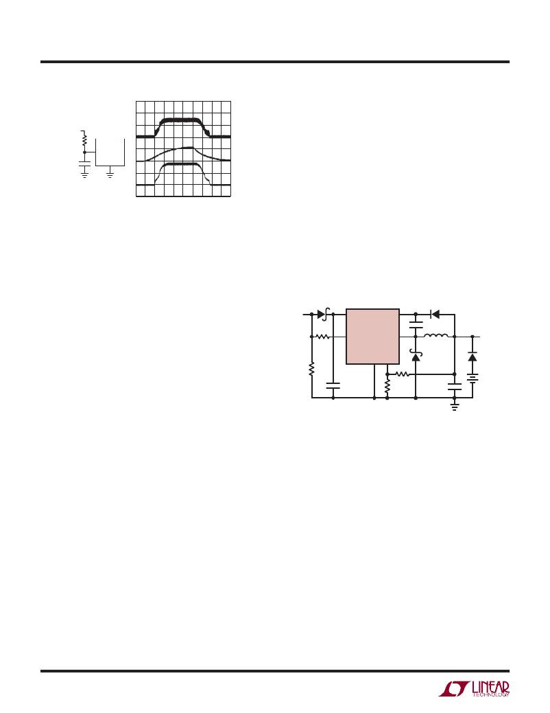
�RUN�
�15k�
�I� L�
�1A/DIV�
�output.� If� the� V� IN� pin� is� allowed� to� ?oat� and� the� RUN/SS�
�pin� is� held� high� (either� by� a� logic� signal� or� because� it� is�
�0.22μF�
�RUN/SS�
�GND�
�V� RUN/SS�
�2V/DIV�
�V� OUT�
�2V/DIV�
�tied� to� V� IN� ),� then� the� LT3680’s� internal� circuitry� will� pull�
�its� quiescent� current� through� its� SW� pin.� This� is� ?ne� if�
�your� system� can� tolerate� a� few� mA� in� this� state.� If� you�
�ground� the� RUN/SS� pin,� the� SW� pin� current� will� drop� to�
�2ms/DIV�
�3680� F07�
�essentially� zero.� However,� if� the� V� IN� pin� is� grounded� while�
�Figure� 7.� To� Soft-Start� the� LT3680,� Add� a� Resisitor�
�and� Capacitor� to� the� RUN/SS� Pin�
�Synchronizing� the� LT3680� oscillator� to� an� external� fre-�
�quency� can� be� done� by� connecting� a� square� wave� (with�
�20%� to� 80%� duty� cycle)� to� the� SYNC� pin.� The� square�
�wave� amplitude� should� have� valleys� that� are� below� 0.3V�
�and� peaks� that� are� above� 0.8V� (up� to� 6V).�
�the� output� is� held� high,� then� parasitic� diodes� inside� the�
�LT3680� can� pull� large� currents� from� the� output� through�
�the� SW� pin� and� the� V� IN� pin.� Figure� 8� shows� a� circuit� that�
�will� run� only� when� the� input� voltage� is� present� and� that�
�protects� against� a� shorted� or� reversed� input.�
�D4�
�MBRS140�
�The� LT3680� will� not� enter� Burst� Mode� at� low� output� loads�
�V� IN�
�V� IN�
�BOOST�
�LT3680�
�while� synchronized� to� an� external� clock,� but� instead� will�
�RUN/SS�
�SW�
�V� OUT�
�skip� pulses� to� maintain� regulation.�
�The� LT3680� may� be� synchronized� over� a� 250kHz� to� 2MHz�
�range.� The� R� T� resistor� should� be� chosen� to� set� the� LT3680�
�switching� frequency� 20%� below� the� lowest� synchronization�
�input.� For� example,� if� the� synchronization� signal� will� be�
�250kHz� and� higher,� the� R� T� should� be� chosen� for� 200kHz.�
�To� assure� reliable� and� safe� operation� the� LT3680� will� only�
�synchronize� when� the� output� voltage� is� near� regulation�
�as� indicated� by� the� PG� ?ag.� It� is� therefore� necessary� to�
�choose� a� large� enough� inductor� value� to� supply� the� required�
�output� current� at� the� frequency� set� by� the� R� T� resistor.� See�
�Inductor� Selection� section.� It� is� also� important� to� note� that�
�slope� compensation� is� set� by� the� R� T� value:� When� the� sync�
�frequency� is� much� higher� than� the� one� set� by� R� T� ,� the� slope�
�compensation� will� be� signi?cantly� reduced� which� may�
�require� a� larger� inductor� value� to� prevent� subharmonic�
�oscillation.�
�Shorted� and� Reversed� Input� Protection�
�If� the� inductor� is� chosen� so� that� it� won’t� saturate� exces-�
�sively,� an� LT3680� buck� regulator� will� tolerate� a� shorted�
�output.� There� is� another� situation� to� consider� in� systems�
�where� the� output� will� be� held� high� when� the� input� to� the�
�LT3680� is� absent.� This� may� occur� in� battery� charging� ap-�
�V� C�
�GND� FB�
�BACKUP�
�3680� F08�
�Figure� 8.� Diode� D4� Prevents� a� Shorted� Input� from�
�Discharging� a� Backup� Battery� Tied� to� the� Output.� It� Also�
�Protects� the� Circuit� from� a� Reversed� Input.� The� LT3680�
�Runs� Only� When� the� Input� is� Present�
�PCB� Layout�
�For� proper� operation� and� minimum� EMI,� care� must� be�
�taken� during� printed� circuit� board� layout.� Figure� 9� shows�
�the� recommended� component� placement� with� trace,�
�ground� plane� and� via� locations.� Note� that� large,� switched�
�currents� ?ow� in� the� LT3680’s� V� IN� and� SW� pins,� the� catch�
�diode� (D1)� and� the� input� capacitor� (C1).� The� loop� formed�
�by� these� components� should� be� as� small� as� possible.� These�
�components,� along� with� the� inductor� and� output� capacitor,�
�should� be� placed� on� the� same� side� of� the� circuit� board,�
�and� their� connections� should� be� made� on� that� layer.� Place�
�a� local,� unbroken� ground� plane� below� these� components.�
�The� SW� and� BOOST� nodes� should� be� as� small� as� possible.�
�Finally,� keep� the� FB� and� V� C� nodes� small� so� that� the� ground�
�3680fb�
�16�
�相关PDF资料 |
PDF描述 |
|---|---|
| LT1534IS-1 | IC REG BOOST ADJ 2A 16SOIC |
| MAX6724AUTZED1+T | IC SUPERVISOR MPU SOT23-6 |
| LT1372HVIS8#TRPBF | IC REG MULTI CONFIG ADJ 8SOIC |
| MAX6724AUTZWD1+T | IC SUPERVISOR MPU SOT23-6 |
| LT1372HVIS8#TR | IC REG MULTI CONFIG ADJ 8SOIC |
相关代理商/技术参数 |
参数描述 |
|---|---|
| LT3680HMSE#PBF | 功能描述:IC REG BUCK ADJ 3.5A 10MSOP RoHS:是 类别:集成电路 (IC) >> PMIC - 稳压器 - DC DC 开关稳压器 系列:- 设计资源:Design Support Tool 标准包装:1 系列:- 类型:升压(升压) 输出类型:固定 输出数:1 输出电压:3V 输入电压:0.75 V ~ 2 V PWM 型:- 频率 - 开关:- 电流 - 输出:100mA 同步整流器:是 工作温度:-40°C ~ 85°C 安装类型:表面贴装 封装/外壳:SOT-23-5 细型,TSOT-23-5 包装:剪切带 (CT) 供应商设备封装:TSOT-23-5 其它名称:AS1323-BTTT-30CT |
| LT3680HMSE#TRPBF | 功能描述:IC REG BUCK ADJ 3.5A 10MSOP RoHS:是 类别:集成电路 (IC) >> PMIC - 稳压器 - DC DC 开关稳压器 系列:- 设计资源:Design Support Tool 标准包装:1 系列:- 类型:升压(升压) 输出类型:固定 输出数:1 输出电压:3V 输入电压:0.75 V ~ 2 V PWM 型:- 频率 - 开关:- 电流 - 输出:100mA 同步整流器:是 工作温度:-40°C ~ 85°C 安装类型:表面贴装 封装/外壳:SOT-23-5 细型,TSOT-23-5 包装:剪切带 (CT) 供应商设备封装:TSOT-23-5 其它名称:AS1323-BTTT-30CT |
| LT3680IDD#PBF | 功能描述:IC REG BUCK ADJ 3.5A 10DFN RoHS:是 类别:集成电路 (IC) >> PMIC - 稳压器 - DC DC 开关稳压器 系列:- 标准包装:250 系列:- 类型:降压(降压) 输出类型:固定 输出数:1 输出电压:1.2V 输入电压:2.05 V ~ 6 V PWM 型:电压模式 频率 - 开关:2MHz 电流 - 输出:500mA 同步整流器:是 工作温度:-40°C ~ 85°C 安装类型:表面贴装 封装/外壳:6-UFDFN 包装:带卷 (TR) 供应商设备封装:6-SON(1.45x1) 产品目录页面:1032 (CN2011-ZH PDF) 其它名称:296-25628-2 |
| LT3680IDD#TRPBF | 功能描述:IC REG BUCK ADJ 3.5A 10DFN RoHS:是 类别:集成电路 (IC) >> PMIC - 稳压器 - DC DC 开关稳压器 系列:- 设计资源:Design Support Tool 标准包装:1 系列:- 类型:升压(升压) 输出类型:固定 输出数:1 输出电压:3V 输入电压:0.75 V ~ 2 V PWM 型:- 频率 - 开关:- 电流 - 输出:100mA 同步整流器:是 工作温度:-40°C ~ 85°C 安装类型:表面贴装 封装/外壳:SOT-23-5 细型,TSOT-23-5 包装:剪切带 (CT) 供应商设备封装:TSOT-23-5 其它名称:AS1323-BTTT-30CT |
| LT3680IDDPBF | 制造商:Linear Technology 功能描述:36V 3.5A 2.4MHz Regulator 75uA DFN10EP |
发布紧急采购,3分钟左右您将得到回复。