- 您现在的位置:买卖IC网 > PDF目录44986 > LT3692EUH#PBF (LINEAR TECHNOLOGY CORP) 5.8 A DUAL SWITCHING CONTROLLER, 2750 kHz SWITCHING FREQ-MAX, PQCC32 PDF资料下载
参数资料
| 型号: | LT3692EUH#PBF |
| 厂商: | LINEAR TECHNOLOGY CORP |
| 元件分类: | 稳压器 |
| 英文描述: | 5.8 A DUAL SWITCHING CONTROLLER, 2750 kHz SWITCHING FREQ-MAX, PQCC32 |
| 封装: | 5 X 5 MM, LEAD FREE, PLASTIC, MO-220WHHD, QFN-32 |
| 文件页数: | 5/36页 |
| 文件大小: | 526K |
| 代理商: | LT3692EUH#PBF |
第1页第2页第3页第4页当前第5页第6页第7页第8页第9页第10页第11页第12页第13页第14页第15页第16页第17页第18页第19页第20页第21页第22页第23页第24页第25页第26页第27页第28页第29页第30页第31页第32页第33页第34页第35页第36页
LT3692
13
3692f
APPLICATIONS INFORMATION
Example.
VIN = 25V, VOUT = 3.3V, IOUT = 2.5A, tON(MIN) = 250ns,
VD = 0.6V, VSW = 0.4V:
Max Frequency
=
3.3
+ 0.6
25 – 0.4
+ 0.6
1
250e-9
~ 600kHz
RT/SYNC ~ 15.8kΩ (Figure 2 )
Input Voltage Range
Once the switching frequency has been determined, the
inputvoltagerangeoftheregulatorcanbedetermined.The
minimuminputvoltageisdeterminedbyeithertheLT3692’s
minimum operating voltage of ~2.8V, or by its maximum
duty cycle. The duty cycle is the fraction of time that the
internal switch is on during a clock cycle. Unlike most
fixed frequency regulators, the LT3692 will not switch off
at the end of each clock cycle if there is sufficient voltage
across the boost capacitor (C3 in Figure 1) to fully satu-
rate the output switch. Forcing switch off for a minimum
time will only occur at the end of a clock cycle when the
boost capacitor needs to be recharged. This operation
has the same effect as lowering the clock frequency for a
fixed off time, resulting in a higher duty cycle and lower
minimum input voltage. The resultant duty cycle depends
on the charging times of the boost capacitor and can be
approximated by the following equation:
DCMAX =
1
+
1
B
where B is 3A divided by the typical boost current from
the Electrical Characteristics table.
This leads to a minimum input voltage of:
VIN(MIN) =
VOUT + VD
DCMAX
– VD + VSW
where VSW is the voltage drop of the internal switch.
Figure 4 shows a typical graph of minimum input voltage
vsloadcurrentforFigure19,the3.3Vand1.8Vapplication.
Table 2. Efficiency and Size Comparisons for Different RRT/SYNC Values, 3.3V Output
FREQUENCY
RT/SYNC
EFFICIENCY
VVIN1/2 = 12V
VIN(MAX)
L*
C*
C + L (Area)
250kHz
5.90kΩ
77.8%
38V
12H
120F
59.8mm2
500kHz
13.0kΩ
81.2%
31V
6.8H
60F
54.6mm2
1000kHz
28.0kΩ
80.5%
16V
3.3H
30F
51.9mm2
1500kHz
44.2kΩ
79.3%
10V
1.5H
22F
46.9mm2
2250kHz
71.5kΩ
76.7%
6.5V
0.82H
15F
19.1mm2
VIN(MAX) is defined as the highest input voltage that maintains constant output voltage ripple.
*Inductor and capacitor values chosen for stability and constant ripple current.
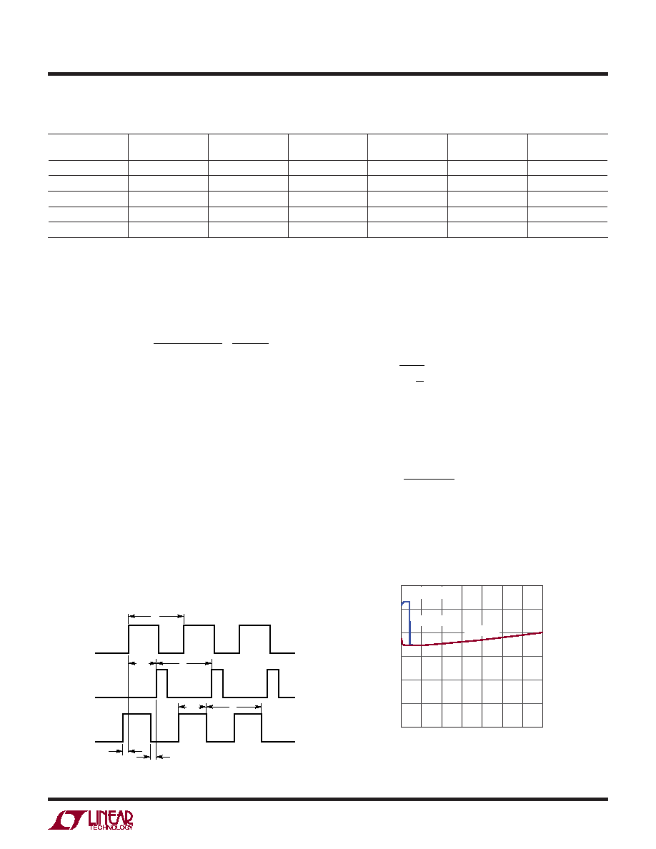
tP
tP/2
tDCLKOSW2
tDCLKOSW1
SW1
SW2
CLKOUT
3692 F03
Figure 3. Timing Diagram RT/SYNC = 28.0k, tP = 1s, VDIV = 0V
Figure 4. Minimum Input Voltage vs Load Current
CURRENT (mA)
0
VOLTAGE
(V)
1
2
3
4
6
500 1000 1500 2000
3692 F04
2500
3500
3000
5
VOUT = 3.3V
START-UP
RUNNING
相关PDF资料 |
PDF描述 |
|---|---|
| LT3724MPFE#TR | SWITCHING CONTROLLER, 225 kHz SWITCHING FREQ-MAX, PDSO16 |
| LT3740EDHC | 0.14 A SWITCHING CONTROLLER, 330 kHz SWITCHING FREQ-MAX, PDSO16 |
| LT3741EFE#PBF | SWITCHING CONTROLLER, 1070 kHz SWITCHING FREQ-MAX, PDSO20 |
| LT3741IFE#TRPBF | SWITCHING CONTROLLER, 1070 kHz SWITCHING FREQ-MAX, PDSO20 |
| LT3741EUF#PBF | SWITCHING CONTROLLER, 1070 kHz SWITCHING FREQ-MAX, PQCC20 |
相关代理商/技术参数 |
参数描述 |
|---|---|
| LT3692IUH#PBF | 功能描述:IC REG BUCK ADJ 3.5A DL 32QFN RoHS:是 类别:集成电路 (IC) >> PMIC - 稳压器 - DC DC 开关稳压器 系列:- 设计资源:Design Support Tool 标准包装:1 系列:- 类型:升压(升压) 输出类型:固定 输出数:1 输出电压:3V 输入电压:0.75 V ~ 2 V PWM 型:- 频率 - 开关:- 电流 - 输出:100mA 同步整流器:是 工作温度:-40°C ~ 85°C 安装类型:表面贴装 封装/外壳:SOT-23-5 细型,TSOT-23-5 包装:剪切带 (CT) 供应商设备封装:TSOT-23-5 其它名称:AS1323-BTTT-30CT |
| LT3692IUH#TRPBF | 功能描述:IC REG BUCK ADJ 3.5A DL 32QFN RoHS:是 类别:集成电路 (IC) >> PMIC - 稳压器 - DC DC 开关稳压器 系列:- 设计资源:Design Support Tool 标准包装:1 系列:- 类型:升压(升压) 输出类型:固定 输出数:1 输出电压:3V 输入电压:0.75 V ~ 2 V PWM 型:- 频率 - 开关:- 电流 - 输出:100mA 同步整流器:是 工作温度:-40°C ~ 85°C 安装类型:表面贴装 封装/外壳:SOT-23-5 细型,TSOT-23-5 包装:剪切带 (CT) 供应商设备封装:TSOT-23-5 其它名称:AS1323-BTTT-30CT |
| LT3692IUHPBF | 制造商:LINER 制造商全称:Linear Technology 功能描述:Monolithic Dual Tracking 3.5A Step-Down Switching Regulator |
| LT3693 | 制造商:LINER 制造商全称:Linear Technology 功能描述:Monolithic Dual Tracking |
| LT36931DD#PBF | 制造商:Linear Technology 功能描述: |
发布紧急采购,3分钟左右您将得到回复。