- 您现在的位置:买卖IC网 > PDF目录44986 > LT3692EUH#PBF (LINEAR TECHNOLOGY CORP) 5.8 A DUAL SWITCHING CONTROLLER, 2750 kHz SWITCHING FREQ-MAX, PQCC32 PDF资料下载
参数资料
| 型号: | LT3692EUH#PBF |
| 厂商: | LINEAR TECHNOLOGY CORP |
| 元件分类: | 稳压器 |
| 英文描述: | 5.8 A DUAL SWITCHING CONTROLLER, 2750 kHz SWITCHING FREQ-MAX, PQCC32 |
| 封装: | 5 X 5 MM, LEAD FREE, PLASTIC, MO-220WHHD, QFN-32 |
| 文件页数: | 9/36页 |
| 文件大小: | 526K |
| 代理商: | LT3692EUH#PBF |
第1页第2页第3页第4页第5页第6页第7页第8页当前第9页第10页第11页第12页第13页第14页第15页第16页第17页第18页第19页第20页第21页第22页第23页第24页第25页第26页第27页第28页第29页第30页第31页第32页第33页第34页第35页第36页
LT3692
17
3692f
APPLICATIONS INFORMATION
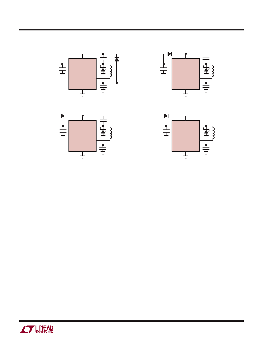
Figure 7. BST Pin Considerations
VIN
VX > VIN + 3V
BST
D2
GND
LT3692
SW
IND
VOUT
VBST – VSW = VX
VBST(MAX) = VX
VX(MIN) = VIN + 3V
VOUT < 3V
3692 F07
VIN
VX = LOWEST VIN
OR VOUT > 3V
BST
D2
GND
LT3692
SW
IND
VOUT
VBST – VSW = VX
VBST(MAX) = VIN + VX
VX(MIN) = 3V
VOUT < 3V
C3
VIN
BST
D2
GND
(7d)
(7c)
(7b)
LT3692
SW
IND
VOUT
VBST – VSW = VIN
VBST(MAX) = 2 VIN
VOUT < 3V
C3
VIN
BST
D2
GND
(7a)
LT3692
SW
IND
VOUT
VBST – VSW = VOUT
VBST(MAX) = VIN + VOUT
VOUT
C3
the switch will not be able to saturate, dropping 1.5V to
2V in conduction.
The minimum input voltage of an LT3692 application is
limited by the minimum operating voltage (<3V) and by
the maximum duty cycle as outlined above. For proper
start-up, the minimum input voltage is also limited by
the boost circuit. If the input voltage is ramped slowly, or
the LT3692 is turned on with its SS pin when the output
is already in regulation, then the boost capacitor may not
be fully charged. Because the boost capacitor is charged
with the energy stored in the inductor, the circuit will rely
on some minimum load current to get the boost circuit
running properly. This minimum load will depend on input
and output voltages, and on the arrangement of the boost
circuit. The Typical Performance Characteristics section
shows plots of the minimum load current to start and to
run as a function of input voltage for 3.3V outputs. In many
cases the discharged output capacitor will present a load
to the switcher which will allow it to start. The plots show
the worst-case situation where VIN is ramping very slowly.
Use a Schottky diode for the lowest start-up voltage.
Outputs Greater Than 6V
For outputs greater than 6V, add a resistor of 1k to 2.5k
across the inductor to damp the discontinuous ringing of
the SW node, preventing unintended SW current. The 12V
output circuit in the Typical Applications section shows
the location of this resistor.
Frequency Compensation
The LT3692 uses current mode control to regulate the
output.Thissimplifiesloopcompensation.Inparticular,the
LT3692 does not require the ESR of the output capacitor
for stability so you are free to use ceramic capacitors to
achieve low output ripple and small circuit size. Frequency
compensation is provided by the components tied to the
VC pin. Generally a capacitor and a resistor in series to
ground determine loop gain. In addition, there is a lower
value capacitor in parallel. This capacitor is not part of
the loop compensation but is used to filter noise at the
switching frequency.
相关PDF资料 |
PDF描述 |
|---|---|
| LT3724MPFE#TR | SWITCHING CONTROLLER, 225 kHz SWITCHING FREQ-MAX, PDSO16 |
| LT3740EDHC | 0.14 A SWITCHING CONTROLLER, 330 kHz SWITCHING FREQ-MAX, PDSO16 |
| LT3741EFE#PBF | SWITCHING CONTROLLER, 1070 kHz SWITCHING FREQ-MAX, PDSO20 |
| LT3741IFE#TRPBF | SWITCHING CONTROLLER, 1070 kHz SWITCHING FREQ-MAX, PDSO20 |
| LT3741EUF#PBF | SWITCHING CONTROLLER, 1070 kHz SWITCHING FREQ-MAX, PQCC20 |
相关代理商/技术参数 |
参数描述 |
|---|---|
| LT3692IUH#PBF | 功能描述:IC REG BUCK ADJ 3.5A DL 32QFN RoHS:是 类别:集成电路 (IC) >> PMIC - 稳压器 - DC DC 开关稳压器 系列:- 设计资源:Design Support Tool 标准包装:1 系列:- 类型:升压(升压) 输出类型:固定 输出数:1 输出电压:3V 输入电压:0.75 V ~ 2 V PWM 型:- 频率 - 开关:- 电流 - 输出:100mA 同步整流器:是 工作温度:-40°C ~ 85°C 安装类型:表面贴装 封装/外壳:SOT-23-5 细型,TSOT-23-5 包装:剪切带 (CT) 供应商设备封装:TSOT-23-5 其它名称:AS1323-BTTT-30CT |
| LT3692IUH#TRPBF | 功能描述:IC REG BUCK ADJ 3.5A DL 32QFN RoHS:是 类别:集成电路 (IC) >> PMIC - 稳压器 - DC DC 开关稳压器 系列:- 设计资源:Design Support Tool 标准包装:1 系列:- 类型:升压(升压) 输出类型:固定 输出数:1 输出电压:3V 输入电压:0.75 V ~ 2 V PWM 型:- 频率 - 开关:- 电流 - 输出:100mA 同步整流器:是 工作温度:-40°C ~ 85°C 安装类型:表面贴装 封装/外壳:SOT-23-5 细型,TSOT-23-5 包装:剪切带 (CT) 供应商设备封装:TSOT-23-5 其它名称:AS1323-BTTT-30CT |
| LT3692IUHPBF | 制造商:LINER 制造商全称:Linear Technology 功能描述:Monolithic Dual Tracking 3.5A Step-Down Switching Regulator |
| LT3693 | 制造商:LINER 制造商全称:Linear Technology 功能描述:Monolithic Dual Tracking |
| LT36931DD#PBF | 制造商:Linear Technology 功能描述: |
发布紧急采购,3分钟左右您将得到回复。