参数资料
| 型号: | LT3693IMSE#TRPBF |
| 厂商: | Linear Technology |
| 文件页数: | 14/24页 |
| 文件大小: | 0K |
| 描述: | IC REG BUCK ADJ 3.5A 10MSOP |
| 标准包装: | 2,500 |
| 类型: | 降压(降压) |
| 输出类型: | 可调式 |
| 输出数: | 1 |
| 输出电压: | 0.79 V ~ 30 V |
| 输入电压: | 3.6 V ~ 36 V |
| PWM 型: | 电流模式 |
| 频率 - 开关: | 200kHz ~ 2.45MHz |
| 电流 - 输出: | 3.5A |
| 同步整流器: | 无 |
| 工作温度: | -40°C ~ 125°C |
| 安装类型: | 表面贴装 |
| 封装/外壳: | 10-TFSOP,10-MSOP(0.118",3.00mm 宽)裸露焊盘 |
| 包装: | 带卷 (TR) |
| 供应商设备封装: | 10-MSOP 裸露焊盘 |
�� �
�
�LT3693�
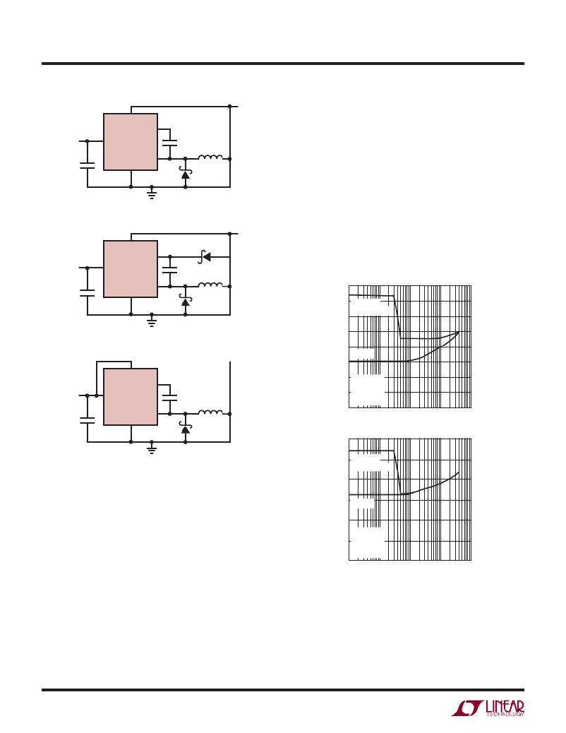
�APPLICATIONS� INFORMATION�
�BD�
�V� OUT�
�is� marginally� adequate� to� support� the� boosted� drive� stage�
�while� using� the� internal� boost� diode.� For� reliable� BOOST� pin�
�V� IN�
�4.7� F�
�V� IN�
�BOOST�
�LT3693�
�SW�
�GND�
�C3�
�operation� with� 2.5V� outputs� use� a� good� external� Schottky�
�diode� (such� as� the� ON� Semi� MBR0540),� and� a� 1μF� boost�
�capacitor� (see� Figure� 4b).� For� lower� output� voltages� the�
�boost� diode� can� be� tied� to� the� input� (Figure� 4c),� or� to�
�another� supply� greater� than� 2.8V.� Tying� BD� to� V� IN� reduces�
�the� maximum� input� voltage� to� 28V.� The� circuit� in� Figure� 4a�
�(4a)� For� V� OUT� >� 2.8V�
�V� OUT�
�is� more� ef?cient� because� the� BOOST� pin� current� and� BD�
�pin� quiescent� current� comes� from� a� lower� voltage� source.�
�You� must� also� be� sure� that� the� maximum� voltage� ratings�
�BD�
�BOOST�
�D2�
�of� the� BOOST� and� BD� pins� are� not� exceeded.�
�V� IN�
�V� IN�
�LT3693�
�C3�
�4.7� F�
�GND�
�SW�
�6.0�
�5.5�
�TO� START�
�(WORST� CASE)�
�5.0�
�(4b)� For� 2.5V� <� V� OUT� <� 2.8V�
�4.5�
�4.0�
�V� OUT�
�3.5�
�TO� RUN�
�V� IN�
�V� IN�
�BD�
�BOOST�
�LT3693�
�C3�
�3.0�
�2.5�
�2.0�
�V� OUT� =� 3.3V�
�T� A� =� 25� C�
�L� =� 8.2� H�
�f� =� 600kHz�
�4.7� F�
�GND�
�SW�
�1�
�10�
�100� 1000�
�LOAD� CURRENT� (mA)�
�10000�
�8.0�
�3693� FO5�
�(4c)� For� V� OUT� <� 2.5V;� V� IN(MAX)� =� 28V�
�7.0�
�TO� START�
�(WORST� CASE)�
�Figure� 4.� Three� Circuits� For� Generating� The� Boost� Voltage�
�6.0�
�BOOST� and� BIAS� Pin� Considerations�
�Capacitor� C3� and� the� internal� boost� Schottky� diode� (see�
�5.0�
�4.0�
�TO� RUN�
�V� OUT� =� 5V�
�the� Block� Diagram)� are� used� to� generate� a� boost� volt-�
�age� that� is� higher� than� the� input� voltage.� In� most� cases�
�a� 0.47μF� capacitor� will� work� well.� Figure� 2� shows� three�
�3.0�
�2.0�
�1�
�T� A� =� 25� C�
�L� =� 8.2� H�
�f� =� 600kHz�
�10�
�100� 1000�
�10000�
�ways� to� arrange� the� boost� circuit.� The� BOOST� pin� must� be�
�more� than� 2.3V� above� the� SW� pin� for� best� ef?ciency.� For�
�LOAD� CURRENT� (mA)�
�3693� F06�
�outputs� of� 3V� and� above,� the� standard� circuit� (Figure� 4a)�
�is� best.� For� outputs� between� 2.8V� and� 3V,� use� a� 1μF� boost�
�Figure� 5.� The� Minimum� Input� Voltage� Depends� on�
�Output� Voltage,� Load� Current� and� Boost� Circuit�
�capacitor.� A� 2.5V� output� presents� a� special� case� because� it�
�3693f�
�14�
�相关PDF资料 |
PDF描述 |
|---|---|
| LT3695HMSE-5#TRPBF | IC REG BUCK 5V 1A 16MSOP |
| LT3710EFE#TRPBF | IC REG CTRLR BUCK PWM 16-TSSOP |
| LT3724EFE#PBF | IC REG CTRLR BST INV PWM 16TSSOP |
| LT3740EDHC#PBF | IC REG CTRLR BUCK PWM CM 16-DFN |
| LT3741EFE#PBF | IC REG CTRLR BUCK PWM CM 20TSSOP |
相关代理商/技术参数 |
参数描述 |
|---|---|
| LT3694 | 制造商:LINER 制造商全称:Linear Technology 功能描述:36V, 2.6A Monolithic Buck |
| LT3694_12 | 制造商:LINER 制造商全称:Linear Technology 功能描述:36V, 2.6A Monolithic Buck |
| LT3694-1 | 制造商:LINER 制造商全称:Linear Technology 功能描述:36V, 2.6A Monolithic Buck |
| LT3694-1EFEPBF | 制造商:LINER 制造商全称:Linear Technology 功能描述:36V, 2.6A Monolithic Buck Regulator With Dual LDO |
| LT3694-1EUFDPBF | 制造商:LINER 制造商全称:Linear Technology 功能描述:36V, 2.6A Monolithic Buck Regulator With Dual LDO |
发布紧急采购,3分钟左右您将得到回复。