参数资料
| 型号: | LT3693IMSE#TRPBF |
| 厂商: | Linear Technology |
| 文件页数: | 16/24页 |
| 文件大小: | 0K |
| 描述: | IC REG BUCK ADJ 3.5A 10MSOP |
| 标准包装: | 2,500 |
| 类型: | 降压(降压) |
| 输出类型: | 可调式 |
| 输出数: | 1 |
| 输出电压: | 0.79 V ~ 30 V |
| 输入电压: | 3.6 V ~ 36 V |
| PWM 型: | 电流模式 |
| 频率 - 开关: | 200kHz ~ 2.45MHz |
| 电流 - 输出: | 3.5A |
| 同步整流器: | 无 |
| 工作温度: | -40°C ~ 125°C |
| 安装类型: | 表面贴装 |
| 封装/外壳: | 10-TFSOP,10-MSOP(0.118",3.00mm 宽)裸露焊盘 |
| 包装: | 带卷 (TR) |
| 供应商设备封装: | 10-MSOP 裸露焊盘 |
�� �
�
�LT3693�
�APPLICATIONS� INFORMATION�
�Shorted� and� Reversed� Input� Protection�
�If� the� inductor� is� chosen� so� that� it� won’t� saturate� exces-�
�sively,� an� LT3693� buck� regulator� will� tolerate� a� shorted�
�output.� There� is� another� situation� to� consider� in� systems�
�where� the� output� will� be� held� high� when� the� input� to� the�
�LT3693� is� absent.� This� may� occur� in� battery� charging� ap-�
�plications� or� in� battery� backup� systems� where� a� battery�
�or� some� other� supply� is� diode� OR-ed� with� the� LT3693’s�
�output.� If� the� V� IN� pin� is� allowed� to� ?oat� and� the� RUN/SS�
�pin� is� held� high� (either� by� a� logic� signal� or� because� it� is�
�tied� to� V� IN� ),� then� the� LT3693’s� internal� circuitry� will� pull�
�its� quiescent� current� through� its� SW� pin.� This� is� ?ne� if�
�your� system� can� tolerate� a� few� mA� in� this� state.� If� you�
�ground� the� RUN/SS� pin,� the� SW� pin� current� will� drop� to�
�essentially� zero.� However,� if� the� V� IN� pin� is� grounded� while�
�the� output� is� held� high,� then� parasitic� diodes� inside� the�
�LT3693� can� pull� large� currents� from� the� output� through�
�the� SW� pin� and� the� V� IN� pin.� Figure� 7� shows� a� circuit� that�
�will� run� only� when� the� input� voltage� is� present� and� that�
�protects� against� a� shorted� or� reversed� input.�
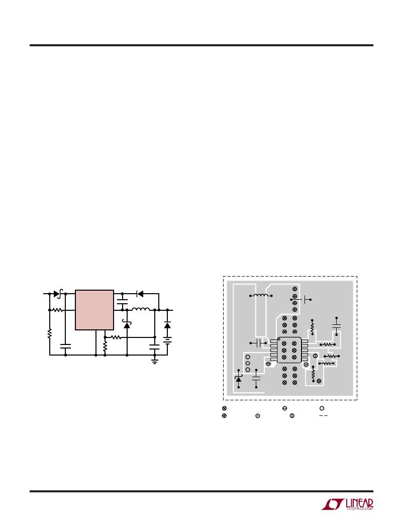
�PCB� Layout�
�For� proper� operation� and� minimum� EMI,� care� must� be�
�taken� during� printed� circuit� board� layout.� Figure� 8� shows�
�the� recommended� component� placement� with� trace,�
�ground� plane� and� via� locations.� Note� that� large,� switched�
�currents� ?ow� in� the� LT3693’s� V� IN� and� SW� pins,� the� catch�
�diode� (D1)� and� the� input� capacitor� (C1).� The� loop� formed�
�by� these� components� should� be� as� small� as� possible.� These�
�components,� along� with� the� inductor� and� output� capacitor,�
�should� be� placed� on� the� same� side� of� the� circuit� board,�
�and� their� connections� should� be� made� on� that� layer.� Place�
�a� local,� unbroken� ground� plane� below� these� components.�
�The� SW� and� BOOST� nodes� should� be� as� small� as� possible.�
�Finally,� keep� the� FB� and� V� C� nodes� small� so� that� the� ground�
�traces� will� shield� them� from� the� SW� and� BOOST� nodes.�
�The� Exposed� Pad� on� the� bottom� of� the� package� must� be�
�soldered� to� ground� so� that� the� pad� acts� as� a� heat� sink.� To�
�keep� thermal� resistance� low,� extend� the� ground� plane� as�
�much� as� possible,� and� add� thermal� vias� under� and� near�
�the� LT3693� to� additional� ground� planes� within� the� circuit�
�board� and� on� the� bottom� side.�
�D4�
�MBRS140�
�V� IN�
�V� IN�
�BOOST�
�L1�
�V� OUT�
�C2�
�LT3693�
�RUN/SS�
�V� C�
�SW�
�V� OUT�
�R� RT�
�C� C�
�GND� FB�
�3693� F08�
�BACKUP�
�D1�
�C1�
�R� C�
�R2�
�R1�
�Figure� 7.� Diode� D4� Prevents� a� Shorted� Input� from�
�Discharging� a� Backup� Battery� Tied� to� the� Output.� It� Also�
�Protects� the� Circuit� from� a� Reversed� Input.� The� LT3693�
�GND�
�R� PG�
�Runs� Only� When� the� Input� is� Present�
�VIAS� TO� LOCAL� GROUND� PLANE�
�VIAS� TO� RUN/SS�
�VIAS� TO� V� IN�
�3693� F09�
�VIAS� TO� V� OUT�
�VIAS� TO� SYNC�
�VIAS� TO� PG�
�OUTLINE� OF� LOCAL�
�GROUND� PLANE�
�Figure� 8.� A� Good� PCB� Layout� Ensures� Proper,� Low� EMI� Operation�
�3693f�
�16�
�相关PDF资料 |
PDF描述 |
|---|---|
| LT3695HMSE-5#TRPBF | IC REG BUCK 5V 1A 16MSOP |
| LT3710EFE#TRPBF | IC REG CTRLR BUCK PWM 16-TSSOP |
| LT3724EFE#PBF | IC REG CTRLR BST INV PWM 16TSSOP |
| LT3740EDHC#PBF | IC REG CTRLR BUCK PWM CM 16-DFN |
| LT3741EFE#PBF | IC REG CTRLR BUCK PWM CM 20TSSOP |
相关代理商/技术参数 |
参数描述 |
|---|---|
| LT3694 | 制造商:LINER 制造商全称:Linear Technology 功能描述:36V, 2.6A Monolithic Buck |
| LT3694_12 | 制造商:LINER 制造商全称:Linear Technology 功能描述:36V, 2.6A Monolithic Buck |
| LT3694-1 | 制造商:LINER 制造商全称:Linear Technology 功能描述:36V, 2.6A Monolithic Buck |
| LT3694-1EFEPBF | 制造商:LINER 制造商全称:Linear Technology 功能描述:36V, 2.6A Monolithic Buck Regulator With Dual LDO |
| LT3694-1EUFDPBF | 制造商:LINER 制造商全称:Linear Technology 功能描述:36V, 2.6A Monolithic Buck Regulator With Dual LDO |
发布紧急采购,3分钟左右您将得到回复。