- 您现在的位置:买卖IC网 > PDF目录10686 > LTC1040CSW#PBF (Linear Technology)IC COMPARATOR LOW PWR DUAL18SOIC PDF资料下载
参数资料
| 型号: | LTC1040CSW#PBF |
| 厂商: | Linear Technology |
| 文件页数: | 10/12页 |
| 文件大小: | 0K |
| 描述: | IC COMPARATOR LOW PWR DUAL18SOIC |
| 标准包装: | 40 |
| 系列: | LTCMOS™ |
| 类型: | 通用 |
| 元件数: | 2 |
| 输出类型: | CMOS,TTL |
| 电压 - 电源,单路/双路(±): | 2.8 V ~ 16 V,±2.8 V ~ 8 V |
| 电压 - 输入偏移(最小值): | 4.5mV @ ±8V |
| 电流 - 输入偏压(最小值): | 300pA @ ±5V |
| 电流 - 静态(最大值): | 3mA |
| 工作温度: | -40°C ~ 85°C |
| 封装/外壳: | 18-SOIC(0.295",7.50mm 宽) |
| 安装类型: | 表面贴装 |
| 包装: | 管件 |
7
LTC1040
1040fa
1A
100mV
APPLICATIO S I FOR ATIO
WU
UU
Offset Voltage Error
The errors due to offset, common mode, power supply
variation, gain and temperature are all included in the
offset voltage specification. This makes it easy to compute
the error when using the LTC1040.
Example: error computation for Figure 4.
Assume: 2.8V
≤ VS ≤ 6V.
Then total worst-case error is:
Note: If source resistance exceeds 10k, bypass
capacitors should be used and the associated errors must
be included.
Pulsed Power (VP-P) Output
It is often desirable to use comparators with resistive
networks such as bridges. Because of the extremely low
power consumption of the LTC1040, the power consumed
by these resistive networks can far exceed that of the
device itself.
At low sample rates the LTC1040 spends most of its time
off. To take advantage of this, a pulsed power (VP-P) output
is provided. VP-P is switched to V+ when the comparator
is on and to a high impedance (open circuit) when the
comparator is off. The ON time is nominally 80
s.
Figure 5 shows the VP-P output circuit.
The VP-P output voltage is not precise (see VP-P Output
Voltage versus Load Current curve). There are two ways
VP-P can be used to power external networks without
excessive errors: (1) ratiometric networks and (2) fast
settling references.
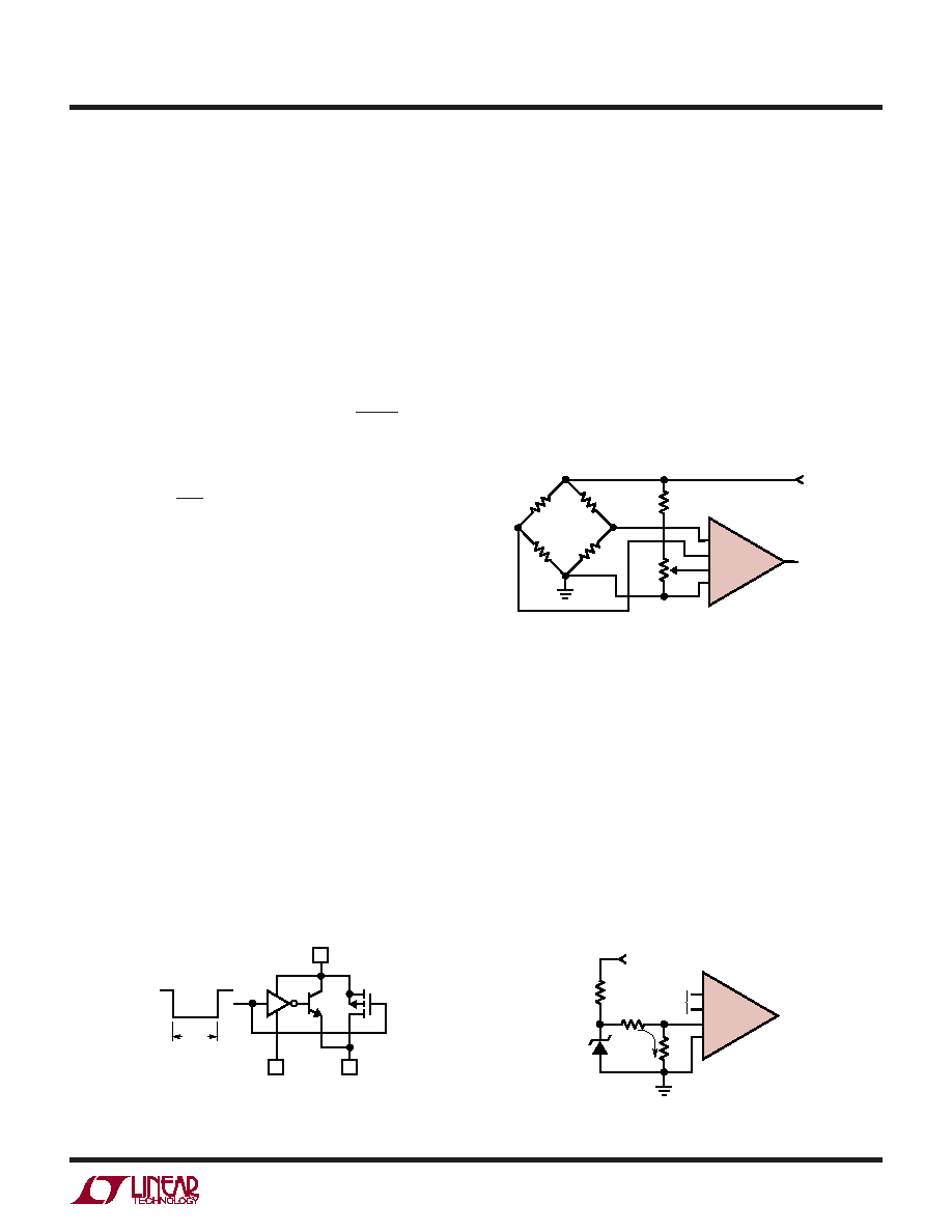
In a ratiometric network, the inputs are all proportional to
VP-P (see Figure 6). Consequently, for small changes, the
absolute value of VP-P does not affect accuracy.
It is critical that the inputs to the LTC1040 completely
settle within 4
s of the start of the comparison cycle and
that they do not change during the 80
s ON time. When
driving resistive networks with VP-P, capacitive loading on
the network should be minimized to meet the 4
s settling
time requirement. It is not recommended that VP-P be used
to drive networks with source impedances, as seen by the
inputs, of greater than 10k
.
In applications where an absolute reference is required,
the VP-P output can be used to drive a fast settling
reference. The LT1009 2.5V reference, ideal in this
application, settles in approximately 2
s (see Figure 7).
The current through R1 must be large enough to supply
the LT1009 minimum bias current (
≈1mA) and the load
current, IL.
LTC1040 AI05
80
s
COMPARATOR ON TIME
18
V+
917
GND
Q1 P1
VP-P
Figure 7. Driving Reference with VP-P Output
Figure 6. Ratiometric Network Driven by VP-P
Figure 5. VP-P Output Switch
=
±6mA
IL (ERROR) = ± (100mV 0.001 + 0.5mV)
↑↑
Tracking Error
VOS
IL (ERROR)% =
100 =
± 0.6%.
6mA
1A
VIN
VTRIP
OUTPUT
VP-P OUTPUT
LTC1040 AI06
–
–+
–
+
1/2
LTC1040
VIN
IL
VP-P OUTPUT
LTC1040 AI07
–
+
1/2
LTC1040
R2
R3
LT1009
R1
相关PDF资料 |
PDF描述 |
|---|---|
| VE-20K-IX-B1 | CONVERTER MOD DC/DC 40V 75W |
| VI-JWR-MY-F3 | CONVERTER MOD DC/DC 7.5V 50W |
| VE-20J-IX-B1 | CONVERTER MOD DC/DC 36V 75W |
| LT1011ACN8 | IC VOLTAGE COMPARATOR 5V 8-DIP |
| AD8561AR-REEL7 | IC COMP 7NS ULTRA-FAST 8-SOIC |
相关代理商/技术参数 |
参数描述 |
|---|---|
| LTC1040M | 制造商:LINER 制造商全称:Linear Technology 功能描述:Dual Micropower Comparator |
| LTC1040MJ | 制造商:LINER 制造商全称:Linear Technology 功能描述:Dual Micropower Comparator |
| LTC1040MJ/883 | 制造商:未知厂家 制造商全称:未知厂家 功能描述:Analog Comparator |
| LTC1041 | 制造商:LINEAR 制造商全称:LINEAR 功能描述:Ultralow Voltage Step-Up Converter and Power Manager |
| LTC1041_09 | 制造商:LINER 制造商全称:Linear Technology 功能描述:BANG-BANG Controller |
发布紧急采购,3分钟左右您将得到回复。