- 您现在的位置:买卖IC网 > PDF目录10686 > LTC1040CSW#PBF (Linear Technology)IC COMPARATOR LOW PWR DUAL18SOIC PDF资料下载
参数资料
| 型号: | LTC1040CSW#PBF |
| 厂商: | Linear Technology |
| 文件页数: | 9/12页 |
| 文件大小: | 0K |
| 描述: | IC COMPARATOR LOW PWR DUAL18SOIC |
| 标准包装: | 40 |
| 系列: | LTCMOS™ |
| 类型: | 通用 |
| 元件数: | 2 |
| 输出类型: | CMOS,TTL |
| 电压 - 电源,单路/双路(±): | 2.8 V ~ 16 V,±2.8 V ~ 8 V |
| 电压 - 输入偏移(最小值): | 4.5mV @ ±8V |
| 电流 - 输入偏压(最小值): | 300pA @ ±5V |
| 电流 - 静态(最大值): | 3mA |
| 工作温度: | -40°C ~ 85°C |
| 封装/外壳: | 18-SOIC(0.295",7.50mm 宽) |
| 安装类型: | 表面贴装 |
| 包装: | 管件 |
6
LTC1040
1040fa
Tracking Error
Tracking error is caused by the ratio error between CIN1
and CIN2 and is expressed as a percentage. For example,
consider Figure 3a with VREF = 1V. Then at null,
Minimizing Comparison Errors
The two differential input voltages, V1 and V2, are con-
verted to charge by the input capacitors CIN1 and CIN2 (see
Figure 2). The charge is summed at the virtual ground
point; if the net charge is positive, the comparator output
is high and if negative, it is low. There is an optimum way
to connect these inputs, in a specific application, to
minimize error.
APPLICATIO S I FOR ATIO
WU
UU
Ignoring internal offset, the LTC1040 will be at its switch-
ing point when:
V1 CIN1 + V2 CIN2 = 0.
Optimum error will be achieved when the differential
voltages, V1 and V2, are individually minimized. Figure 3
shows two ways to connect the LTC1040 to compare an
input voltage, VIN, to a reference voltage, VREF. Using the
above equation, each method will be at null when:
(a)
(VREF – 0V) CIN1 – (0V – VIN) CIN2 = 0
or VIN = VREF (CIN1/CIN2)
(b) (VREF – VIN) CIN1 – (0V – 0V) CIN2 = 0
or VIN = VREF.
Notice that in method (a) the null point depends on the
ratio of CIN1/CIN2, but method (b) is independent of this
ratio. Also, because method (b) has zero differential input
voltage, the errors due to finite input resistance are
negligible. The LTC1040 has a high accuracy capacitor
array and even the non-optimum connection will only
result in
± 0.1% more error, worst-case compared to the
optimum connection.
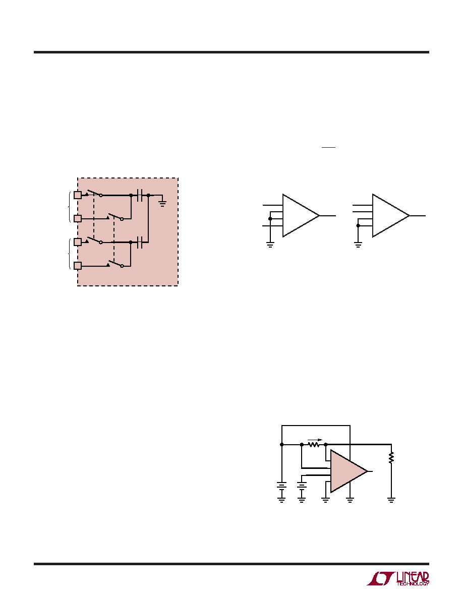
LTC1040 AI02
CIN1
VIRTUAL
GROUND
LTC1040 DUAL DIFFERENTIAL INPUT
S1
S2
+
–
+
–
V1
V2
CIN2
Figure 2. Dual Differential Equivalent Input Circuit
Common Mode Range
The input switches of the LTC1040 are capable of
switching to either the V+ or V– supply. This means that the
input common mode range includes both supply rails.
Many applications, not feasible with conventional com-
parators, are possible with the LTC1040. In the load
current detector shown in Figure 4, a 0.1
resistor is used
to sense the current in the V+ supply. This application
requires the dual differential input and common mode
capabilities of the LTC1040.
Figure 4. Load Current Detector
VIN = VREF
CIN1
CIN2
= 1V
± 1mV
Figure 3. Two Ways to Do It
VREF
VIN
VREF
VIN
LTC1040 TA03
–
+
–
+
(a) OK
(b) Optimum
because CIN1 is guaranteed to equal CIN2 to within 0.1%.
VS
RL
LTC1040 AI04
IL
100mV
–
+
0.1
OUT
1/2
LTC1040
OUT = HI IF IL > 1A
OUT = LO IF IL < 1A
相关PDF资料 |
PDF描述 |
|---|---|
| VE-20K-IX-B1 | CONVERTER MOD DC/DC 40V 75W |
| VI-JWR-MY-F3 | CONVERTER MOD DC/DC 7.5V 50W |
| VE-20J-IX-B1 | CONVERTER MOD DC/DC 36V 75W |
| LT1011ACN8 | IC VOLTAGE COMPARATOR 5V 8-DIP |
| AD8561AR-REEL7 | IC COMP 7NS ULTRA-FAST 8-SOIC |
相关代理商/技术参数 |
参数描述 |
|---|---|
| LTC1040M | 制造商:LINER 制造商全称:Linear Technology 功能描述:Dual Micropower Comparator |
| LTC1040MJ | 制造商:LINER 制造商全称:Linear Technology 功能描述:Dual Micropower Comparator |
| LTC1040MJ/883 | 制造商:未知厂家 制造商全称:未知厂家 功能描述:Analog Comparator |
| LTC1041 | 制造商:LINEAR 制造商全称:LINEAR 功能描述:Ultralow Voltage Step-Up Converter and Power Manager |
| LTC1041_09 | 制造商:LINER 制造商全称:Linear Technology 功能描述:BANG-BANG Controller |
发布紧急采购,3分钟左右您将得到回复。