- 您现在的位置:买卖IC网 > PDF目录10686 > LTC1040CSW#PBF (Linear Technology)IC COMPARATOR LOW PWR DUAL18SOIC PDF资料下载
参数资料
| 型号: | LTC1040CSW#PBF |
| 厂商: | Linear Technology |
| 文件页数: | 8/12页 |
| 文件大小: | 0K |
| 描述: | IC COMPARATOR LOW PWR DUAL18SOIC |
| 标准包装: | 40 |
| 系列: | LTCMOS™ |
| 类型: | 通用 |
| 元件数: | 2 |
| 输出类型: | CMOS,TTL |
| 电压 - 电源,单路/双路(±): | 2.8 V ~ 16 V,±2.8 V ~ 8 V |
| 电压 - 输入偏移(最小值): | 4.5mV @ ±8V |
| 电流 - 输入偏压(最小值): | 300pA @ ±5V |
| 电流 - 静态(最大值): | 3mA |
| 工作温度: | -40°C ~ 85°C |
| 封装/外壳: | 18-SOIC(0.295",7.50mm 宽) |
| 安装类型: | 表面贴装 |
| 包装: | 管件 |
5
LTC1040
1040fa
The LTC1040 uses sampled data techniques to achieve its
unique characteristics. Some of the experience acquired
using classic linear comparators does not apply to this
circuit, so a brief description of internal operation is
essential to proper application.
The most obvious difference between the LTC1040 and
other comparators is the dual differential input structure.
Functionally, when the sum of inputs is positive, the
comparator output is high and when the sum of the inputs
is negative, the output is low. This unique input structure
is achieved with CMOS switches and a precision capacitor
array. Because of the switching nature of the inputs, the
concept of input current and input impedance needs to be
examined.
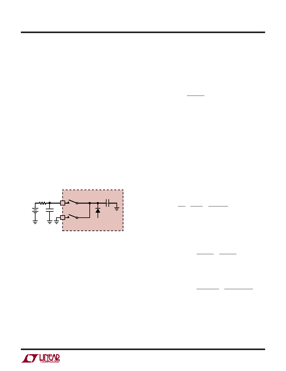
The equivalent input circuit is shown in Figure 1. Here, the
input is being driven by a resistive source, RS, with a
bypass capacitor, CS. The bypass capacitor may or may
not be needed, depending on the size of the source
resistance and the magnitude of the input voltage, VIN.
APPLICATIO S I FOR ATIO
WU
UU
Figure 1. Equivalent Input Circuit
VIN
RS
CS
LTC1040 AI01
S1
S2
CIN
≈ 33pF
V–
LTC1040 DIFFERENTIAL INPUT
+
–
For RS < 1Ok
Assuming CS is zero, the input capacitor, CIN, charges to
VIN with a time constant of RS CIN. When RS is too large,
CIN does not have a chance to fully charge during the
sampling interval (
≈ 80s) and errors will result. If RS
exceeds 10k
, a bypass capacitor is necessary to mini-
mize errors.
For RS > 1Ok
For RS greater than 10k, CIN cannot fully charge and a
bypass capacitor, CS, is needed. When switch S1 closes,
charge is shared between CS and CIN. The change in
voltage on CS because of this charge sharing is:
V = VIN
CIN
CIN + CS
RIN =
VIN
IIN
=
1
fS CIN
=
1
fS 33pF
This represents an error and can be made arbitrarily small
by increasing CS.
With the addition of CS, a second error term caused by the
finite input resistance of the LTC1040 must be considered.
Switches S1 and S2 alternately open and close, charging
and discharging CIN between VIN and ground. The
alternate charge and discharge of CIN causes a current to
flow into the positive input and out of the negative input.
The magnitude of this current is:
IIN = q fS = VIN CIN fS
where fS is the sampling frequency. Because the input
current is directly proportional to input voltage, the LTC1040
can be said to have an average input resistance of:
Notice that most of the error is caused by RIN. If the
sampling frequency is reduced to 1Hz, the voltage error is
reduced to 66
V.
(see typical curve of Input Resistance vs Sampling Fre-
quency). A voltage divider is set up between RS and RIN
causing error.
The input voltage error caused by these two effects is:
VERROR = VIN
Example: fS = 10Hz, RS = 1M,
CS = 1F, VIN = 1V
()
CIN
CIN + CS
+
RS
RS + RIN
VERROR = 1V
= 33
V + 330V = 363V.
()
33 10–12
106
1 10 –6
106 + 3 109
+
相关PDF资料 |
PDF描述 |
|---|---|
| VE-20K-IX-B1 | CONVERTER MOD DC/DC 40V 75W |
| VI-JWR-MY-F3 | CONVERTER MOD DC/DC 7.5V 50W |
| VE-20J-IX-B1 | CONVERTER MOD DC/DC 36V 75W |
| LT1011ACN8 | IC VOLTAGE COMPARATOR 5V 8-DIP |
| AD8561AR-REEL7 | IC COMP 7NS ULTRA-FAST 8-SOIC |
相关代理商/技术参数 |
参数描述 |
|---|---|
| LTC1040M | 制造商:LINER 制造商全称:Linear Technology 功能描述:Dual Micropower Comparator |
| LTC1040MJ | 制造商:LINER 制造商全称:Linear Technology 功能描述:Dual Micropower Comparator |
| LTC1040MJ/883 | 制造商:未知厂家 制造商全称:未知厂家 功能描述:Analog Comparator |
| LTC1041 | 制造商:LINEAR 制造商全称:LINEAR 功能描述:Ultralow Voltage Step-Up Converter and Power Manager |
| LTC1041_09 | 制造商:LINER 制造商全称:Linear Technology 功能描述:BANG-BANG Controller |
发布紧急采购,3分钟左右您将得到回复。