参数资料
| 型号: | LTC1051CN8 |
| 厂商: | Linear Technology |
| 文件页数: | 13/16页 |
| 文件大小: | 0K |
| 描述: | IC OPAMP CHOPR-STBL DUAL 8-DIP |
| 标准包装: | 50 |
| 放大器类型: | 断路器(零漂移) |
| 电路数: | 2 |
| 转换速率: | 4 V/µs |
| 增益带宽积: | 2.5MHz |
| 电流 - 输入偏压: | 15pA |
| 电压 - 输入偏移: | 0.5µV |
| 电流 - 电源: | 1mA |
| 电压 - 电源,单路/双路(±): | 4.75 V ~ 16 V,±2.38 V ~ 8 V |
| 工作温度: | 0°C ~ 70°C |
| 安装类型: | 通孔 |
| 封装/外壳: | 8-DIP(0.300",7.62mm) |
| 供应商设备封装: | 8-PDIP |
| 包装: | 管件 |
LTC1051/LTC1053
6
10513fa
ACHIEVING PICOAMPERE/MICROVOLT PERFORMANCE
Picoamperes
In order to realize the picoampere level of accuracy of the
LTC1051/LTC1053, proper care must be exercised. Leak-
age currents in circuitry external to the amplifier can
significantly degrade performance. High quality insulation
should be used (e.g., Teflon, Kel-F); cleaning of all insulat-
ing surfaces to remove fluxes and other residues will
probably be necessary —particularly for high temperature
performance. Surface coating may be necessary to provide
a moisture barrier in high humidity environments.
Board leakage can be minimized by encircling the input
connections with a guard ring operated at a potential close
to that of the inputs: in inverting configurations, the guard
ring should be tied to ground; in noninverting connections,
to the inverting input. Guarding both sides of the printed
circuit board is required. Bulk leakage reduction depends
on the guard ring width.
Microvolts
Thermocouple effects must be considered if the LTC1051/
LTC1053’s ultra low drift op amps are to be fully utilized.
Any connection of dissimilar metals forms a thermoelec-
tric junction producing an electric potential which varies
with temperature (Seebeck effect.) As temperature sen-
sors, thermocouples exploit this phenomenon to produce
useful information. In low drift amplifier circuits, this effect
is a primary source of error.
Connectors, switches, relay contacts, sockets, resistors,
solder, and even copper wire are all candidates for thermal
EMF generation. Junctions of copper wire from different
manufacturers can generate thermal EMFs of 200nV/°C—
4 times the maximum drift specification of the LTC1051/
LTC1053. The copper/kovar junction, formed when wire or
printed circuit traces contact a package lead, has a thermal
EMF of approximately 35V/°C—700 times the maximum
drift specification of the LTC1051/LTC1053.
Minimizing thermal EMF-induced errors is possible if
judicious attention is given to circuit board layout and
component selection. It is good practice to minimize the
number of junctions in the amplifier’s input signal path.
Avoid connectors, sockets, switches and relays where
possible. In instances where this is not possible, attempt
to balance the number and type of junctions so that
differential cancellation occurs. Doing this may involve
deliberately introducing junctions to offset unavoidable
junctions.
When connectors, switches, relays and/or sockets are
necessary, they should be selected for low thermal EMF
activity. The same techniques of thermally balancing and
coupling the matching junctions are effective in reducing
the thermal EMF errors of these components.
Resistors are another source of thermal EMF errors.
Table 1 shows the thermal EMF generated for different
resistors. The temperature gradient across the resistor is
important, not the ambient temperature. There are two
junctions formed at each end of the resistor and if these
junctions are at the same temperature, their thermal EMFs
will cancel each other. The thermal EMF numbers are
approximate and vary with resistor value. High values give
higher thermal EMF.
Table 1. Resistor Thermal EMF
RESISTOR TYPE
THERMAL EMF/°C GRADIENT
Tin Oxide
~mV/°C
Carbon Composition
~450V/°C
Metal Film
~20V/°C
Wire Wound
Evenohm
~2V/°C
Manganin
~2V/°C
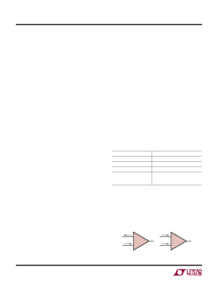
Input Bias Current, Clock Feedthrough
At ambient temperatures below 60°C, the input bias cur-
rent of the LTC1051/LTC1053 op amps’ is dominated by
the small amount of charge injection occurring during the
sampling and holding of the op amps’ input offset voltage.
The average value of the resulting current pulses is 10pA
to 15pA with sign convention shown in Figure 1.
Figure 1. LTC1051 Bias Current
–
+
–
+
1/2
LTC1051
1/2
LTC1051
TA < 60°CTA > 85°C
IB
+
IB
–
IB
+
IB
–
1051/53 F01
(a)
(b)
APPLICATIO S I FOR ATIO
WU
UU
相关PDF资料 |
PDF描述 |
|---|---|
| AD5750-1BCPZ-REEL7 | IC CURR/VOLT OUT DVR 32LFCSP |
| AD5750BCPZ-REEL7 | IC CURR/VOLT OUT DVR 32LFCSP |
| 9-146309-0-39 | CONN HEADR BRKWAY .100 78POS R/A |
| 2035-35-A | GAS DISCHARGE TUBE MINI 2 POLE |
| 2035-30-SM | GAS DISCHARGE TUBE MINI 2 POLE |
相关代理商/技术参数 |
参数描述 |
|---|---|
| LTC1051CN8#PBF | 功能描述:IC OPAMP CHOPR-STBL DUAL 8-DIP RoHS:是 类别:集成电路 (IC) >> Linear - Amplifiers - Instrumentation 系列:- 标准包装:2,500 系列:- 放大器类型:通用 电路数:4 输出类型:- 转换速率:0.6 V/µs 增益带宽积:1MHz -3db带宽:- 电流 - 输入偏压:45nA 电压 - 输入偏移:2000µV 电流 - 电源:1.4mA 电流 - 输出 / 通道:40mA 电压 - 电源,单路/双路(±):3 V ~ 32 V,±1.5 V ~ 16 V 工作温度:0°C ~ 70°C 安装类型:表面贴装 封装/外壳:14-TSSOP(0.173",4.40mm 宽) 供应商设备封装:14-TSSOP 包装:带卷 (TR) 其它名称:LM324ADTBR2G-NDLM324ADTBR2GOSTR |
| LTC1051CN8PBF | 制造商:Linear Technology 功能描述:Dual precision op amp,LTC1051CN8 DIP8 |
| LTC1051CS | 制造商:Linear Technology 功能描述:IC OP AMP DUAL CMOS 1051 SOIC16 |
| LTC1051CS#PBF | 制造商:Linear Technology 功能描述:OP AMP DUAL CMOS 1051 NSOIC16 |
| LTC1051CSW | 功能描述:IC OPAMP CHOPR-STBL DUAL 16SOIC RoHS:否 类别:集成电路 (IC) >> Linear - Amplifiers - Instrumentation 系列:- 标准包装:50 系列:- 放大器类型:J-FET 电路数:2 输出类型:- 转换速率:13 V/µs 增益带宽积:3MHz -3db带宽:- 电流 - 输入偏压:65pA 电压 - 输入偏移:3000µV 电流 - 电源:1.4mA 电流 - 输出 / 通道:- 电压 - 电源,单路/双路(±):7 V ~ 36 V,±3.5 V ~ 18 V 工作温度:-40°C ~ 85°C 安装类型:通孔 封装/外壳:8-DIP(0.300",7.62mm) 供应商设备封装:8-PDIP 包装:管件 |
发布紧急采购,3分钟左右您将得到回复。