参数资料
| 型号: | LTC1051CN8 |
| 厂商: | Linear Technology |
| 文件页数: | 2/16页 |
| 文件大小: | 0K |
| 描述: | IC OPAMP CHOPR-STBL DUAL 8-DIP |
| 标准包装: | 50 |
| 放大器类型: | 断路器(零漂移) |
| 电路数: | 2 |
| 转换速率: | 4 V/µs |
| 增益带宽积: | 2.5MHz |
| 电流 - 输入偏压: | 15pA |
| 电压 - 输入偏移: | 0.5µV |
| 电流 - 电源: | 1mA |
| 电压 - 电源,单路/双路(±): | 4.75 V ~ 16 V,±2.38 V ~ 8 V |
| 工作温度: | 0°C ~ 70°C |
| 安装类型: | 通孔 |
| 封装/外壳: | 8-DIP(0.300",7.62mm) |
| 供应商设备封装: | 8-PDIP |
| 包装: | 管件 |
LTC1051/LTC1053
10
10513fa
SYSTEM BUSY, ONLY ABORT COMMANDS ALLOWED
RANGE: 11dBV
STATUS: PAUSED
20dBV
15dB
/DIV
–100
CENTER: 10 000Hz
X: 5475Hz
BW: 95.485Hz
Y: –58.05dBV
SPAN: 10 000Hz
fIN =10kHz
6fCLK – fIN
68dB
–
+
1/2
LTC1051
1051/53 F07
R1
100
R2
10k
90mVP-P
10kHz
0.1F
50pF
5V
–5V
VOUT
RL (LOAD RESISTANCE,)
V
OUT
±
SWING
(
±
V)
1051/53 G08
01k 2k3k
4k
5k
6k 7k
8k 9k 10k
NEGATIVE SWING
POSITIVE SWING
VS = ±8V, TA ≤85°C
VS = ±5V, TA ≤85°C
VS = ±2.5V, TA ≤85°C
10
9
8
7
6
5
4
3
2
1
0
INVERTING CLOSED-LOOP GAIN
1
OUTPUT
SIGNAL
TO
ALIAS
SIGNAL(S)
RATIO
(dB)
100
10
1051/53 G09
90
80
70
60
50
40
30
20
10
VS = ±5V
fIN ≤10kHz
5. For unity-gain inverting configuration, all the alias
frequencies are 80dB to 84dB down from the output signal
(Figures 6a, 6b). Combined with excellent THD under wide
swing, the LTC1051/LTC1053 op amps make efficient
unity gain inverters.
For gain higher than –1, the “signal to alias” ratio de-
creases at an approximate rate of –6dB per decade of
closed-loop gain (Figure 9).
6. For closed-loop gains of –10 or higher, the “signal to
alias” ratio degrades when the value of the feedback gain
setting resistor increases beyond 50k. For instance, the
68dB value of Figure 7 decreases to 56dB if a (1k, 100k)
resistor set is used to set the gain of –100.
7. When the LTC1051/LTC1053 are used as noninverting
amplifiers, all the previous approximate rules of thumb
apply with the following exceptions: when the closed-loop
gain is 10(V/V) and below, the “signal to alias” ratio is 1dB
to 3dB less than the inverting case; when the closed-loop
gain is 100(V/V), the degradation can be up to 9dB,
especially when the input signal is much higher than the
clock frequency (i.e. fIN = 10kHz).
8. The signal/alias ratio performance improves when the
op amp has bandlimited loop gain.
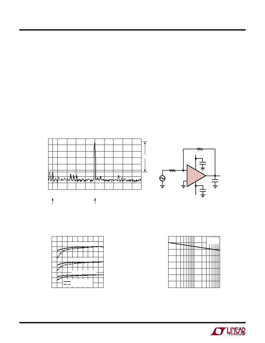
Figure 7. Output Voltage Spectrum of 1/2 LTC1051 Operating as an Inverting Amplifier with a Gain of –100 and
Amplifiying a 90mVP-P, 10kHz Input Signal. With a 9VP-P Output Swing the Measured 2nd Harmonic (20kHz)
was 75 Down from the 10kHz Input Signal
Figure 8. Output Voltage Swing vs Load
Figure 9. Signal to Alias Ratio vs
Closed-Loop Gain
APPLICATIO S I FOR ATIO
WU
UU
相关PDF资料 |
PDF描述 |
|---|---|
| AD5750-1BCPZ-REEL7 | IC CURR/VOLT OUT DVR 32LFCSP |
| AD5750BCPZ-REEL7 | IC CURR/VOLT OUT DVR 32LFCSP |
| 9-146309-0-39 | CONN HEADR BRKWAY .100 78POS R/A |
| 2035-35-A | GAS DISCHARGE TUBE MINI 2 POLE |
| 2035-30-SM | GAS DISCHARGE TUBE MINI 2 POLE |
相关代理商/技术参数 |
参数描述 |
|---|---|
| LTC1051CN8#PBF | 功能描述:IC OPAMP CHOPR-STBL DUAL 8-DIP RoHS:是 类别:集成电路 (IC) >> Linear - Amplifiers - Instrumentation 系列:- 标准包装:2,500 系列:- 放大器类型:通用 电路数:4 输出类型:- 转换速率:0.6 V/µs 增益带宽积:1MHz -3db带宽:- 电流 - 输入偏压:45nA 电压 - 输入偏移:2000µV 电流 - 电源:1.4mA 电流 - 输出 / 通道:40mA 电压 - 电源,单路/双路(±):3 V ~ 32 V,±1.5 V ~ 16 V 工作温度:0°C ~ 70°C 安装类型:表面贴装 封装/外壳:14-TSSOP(0.173",4.40mm 宽) 供应商设备封装:14-TSSOP 包装:带卷 (TR) 其它名称:LM324ADTBR2G-NDLM324ADTBR2GOSTR |
| LTC1051CN8PBF | 制造商:Linear Technology 功能描述:Dual precision op amp,LTC1051CN8 DIP8 |
| LTC1051CS | 制造商:Linear Technology 功能描述:IC OP AMP DUAL CMOS 1051 SOIC16 |
| LTC1051CS#PBF | 制造商:Linear Technology 功能描述:OP AMP DUAL CMOS 1051 NSOIC16 |
| LTC1051CSW | 功能描述:IC OPAMP CHOPR-STBL DUAL 16SOIC RoHS:否 类别:集成电路 (IC) >> Linear - Amplifiers - Instrumentation 系列:- 标准包装:50 系列:- 放大器类型:J-FET 电路数:2 输出类型:- 转换速率:13 V/µs 增益带宽积:3MHz -3db带宽:- 电流 - 输入偏压:65pA 电压 - 输入偏移:3000µV 电流 - 电源:1.4mA 电流 - 输出 / 通道:- 电压 - 电源,单路/双路(±):7 V ~ 36 V,±3.5 V ~ 18 V 工作温度:-40°C ~ 85°C 安装类型:通孔 封装/外壳:8-DIP(0.300",7.62mm) 供应商设备封装:8-PDIP 包装:管件 |
发布紧急采购,3分钟左右您将得到回复。