- 您现在的位置:买卖IC网 > PDF目录15503 > LTC1147CS8-5#PBF (Linear Technology)IC REG CTRLR BUCK PWM CM 8-SOIC PDF资料下载
参数资料
| 型号: | LTC1147CS8-5#PBF |
| 厂商: | Linear Technology |
| 文件页数: | 10/16页 |
| 文件大小: | 0K |
| 描述: | IC REG CTRLR BUCK PWM CM 8-SOIC |
| 标准包装: | 100 |
| PWM 型: | 电流模式 |
| 输出数: | 1 |
| 占空比: | 100% |
| 电源电压: | 3.5 V ~ 14 V |
| 降压: | 是 |
| 升压: | 无 |
| 回扫: | 无 |
| 反相: | 无 |
| 倍增器: | 无 |
| 除法器: | 无 |
| Cuk: | 无 |
| 隔离: | 无 |
| 工作温度: | 0°C ~ 70°C |
| 封装/外壳: | 8-SOIC(0.154",3.90mm 宽) |
| 包装: | 管件 |
| 产品目录页面: | 1332 (CN2011-ZH PDF) |
�� �
�
�LTC1147-3.3�
�LTC1147-5/LTC1147L�
�APPLICATIO� S� I� FOR� ATIO�
�Optimum� efficiency� is� obtained� by� making� the� ESR� equal�
�to� R� SENSE� .� As� the� ESR� is� increased� up� to� 2R� SENSE� ,� the�
�efficiency� degrades� by� less� than� 1%.� If� the� ESR� is� greater�
�than� 2R� SENSE� ,� the� voltage� ripple� on� the� output� capacitor�
�will� prematurely� trigger� Burst� Mode� operation,� resulting� in�
�disruption� of� continuous� mode� and� an� efficiency� hit� which�
�can� be� several� percent.�
�Manufacturers� such� as� Nichicon� and� United� Chemicon�
�should� be� considered� for� high� performance� capacitors.�
�The� OS-CON� semiconductor� dielectric� capacitor� available�
�from� Sanyo� has� the� lowest� ESR/size� ratio� of� any� aluminum�
�electrolytic� at� a� somewhat� higher� price.� Once� the� ESR�
�requirement� for� C� OUT� has� been� met,� the� RMS� current�
�rating� generally� far� exceeds� the� I� RIPPLE(P-P)� requirement.�
�In� surface� mount� applications� multiple� capacitors� may�
�have� to� be� paralleled� to� meet� the� capacitance,� ESR� or� RMS�
�current� handling� requirements� of� the� application.� Alumi-�
�num� electrolytic� and� dry� tantalum� capacitors� are� both�
�available� in� surface� mount� configurations.� In� the� case� of�
�tantalum,� it� is� critical� that� the� capacitors� are� surge� tested�
�for� use� in� switching� power� supplies.� An� excellent� choice�
�is� the� AVX� TPS� series� of� surface� mount� tantalums,� avail-�
�able� in� case� heights� ranging� from� 2mm� to� 4mm.� For�
�example,� if� 200� μ� F/10V� is� called� for� in� an� application�
�requiring� 3mm� height,� two� AVX� 100� μ� F/10V� (P/N� TPSD�
�107K010)� could� be� used.� Consult� the� manufacturer� for�
�other� specific� recommendations.�
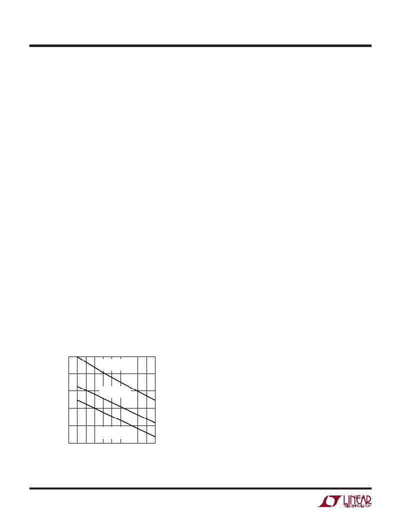
�At� low� supply� voltages,� a� minimum� capacitance� at� C� OUT� is�
�needed� to� prevent� an� abnormal� low� frequency� operating�
�mode� (see� Figure� 4).� When� C� OUT� is� made� too� small,� the�
�output� ripple� at� low� frequencies� will� be� large� enough� to� trip�
�the� voltage� comparator.� This� causes� Burst� Mode� opera-�
�tion� to� be� activated� when� the� LTC1147� series� would�
�normally� be� in� continuous� operation.� The� effect� is� most�
�pronounced� with� low� values� of� R� SENSE� and� can� be� im-�
�proved� by� operating� at� higher� frequencies� with� lower�
�values� of� L.� The� output� remains� in� regulation� at� all� times.�
�Checking� Transient� Response�
�The� regulator� loop� response� can� be� checked� by� looking�
�at� the� load� transient� response.� Switching� regulators�
�take� several� cycles� to� respond� to� a� step� in� DC� (resistive)�
�load� current.� When� a� load� step� occurs,� V� OUT� shifts� by� an�
�amount� equal� to� ?� I� LOAD� (ESR),� where� ESR� is� the� effec-�
�tive� series� resistance� of� C� OUT� .� ?� I� LOAD� also� begins� to�
�charge� or� discharge� C� OUT� until� the� regulator� loop� adapts�
�to� the� current� change� and� returns� V� OUT� to� its� steady�
�state� value.� During� this� recovery� time� V� OUT� can� be�
�monitored� for� overshoot� or� ringing� which� would� indi-�
�cate� a� stability� problem.� The� external� components� shown�
�in� the� Figure� 1� circuit� will� prove� adequate� compensation�
�for� most� applications.�
�A� second,� more� severe� transient� is� caused� by� switching�
�in� loads� with� large� (>1� μ� F)� supply� bypass� capacitors.� The�
�discharged� bypass� capacitors� are� effectively� put� in� par-�
�allel� with� C� OUT� ,� causing� a� rapid� drop� in� V� OUT� .� No� regulator�
�can� deliver� enough� current� to� prevent� this� problem� if� the�
�load� switch� resistance� is� low� and� it� is� driven� quickly.� The�
�only� solution� is� to� limit� the� rise� time� of� the� switch� drive� so�
�1000�
�800�
�600�
�400�
�L� =� 50� μ� H�
�R� SENSE� =� 0.02� ?�
�L� =� 25� μ� H�
�R� SENSE� =� 0.02� ?�
�that� the� load� rise� time� is� limited� to� approximately�
�(25)C� LOAD� .� Thus� a� 10� μ� F� capacitor� would� require� a� 250� μ� s�
�rise� time,� limiting� the� charging� current� to� about� 200mA.�
�Efficiency� Considerations�
�The� percent� efficiency� of� a� switching� regulator� is� equal� to�
�the� output� power� divided� by� the� input� power� times� 100%.�
�200�
�0�
�0�
�1�
�L� =� 50� μ� H�
�R� SENSE� =� 0.05� ?�
�2� 3�
�(V� IN� –� V� OUT� )� VOLTAGE� (V)�
�4�
�5�
�It� is� often� useful� to� analyze� individual� losses� to� determine�
�what� is� limiting� the� efficiency� and� which� change� would�
�produce� the� most� improvement.� Percent� efficiency� can� be�
�expressed� as:�
�LTC1147� ?� F04�
�%Efficiency� =� 100%� –� (L1� +� L2� +� L3� +� ...)�
�Figure� 4.� Minimum� Value� of� C� OUT�
�sn1147� 1147fds�
�10�
�相关PDF资料 |
PDF描述 |
|---|---|
| SPD62-103M | INDUCTOR PWR SHIELDED 10.0UH SMD |
| LTC3830-1ES8#PBF | IC REG CTRLR BUCK PWM VM 8-SOIC |
| LTC3830-1ES8 | IC REG CTRLR BUCK PWM VM 8-SOIC |
| LTC3823IGN#PBF | IC REG CTRLR BUCK PWM CM 28-SSOP |
| SPD62-682M | INDUCTOR PWR SHIELDED 6.80UH SMD |
相关代理商/技术参数 |
参数描述 |
|---|---|
| LTC1147HVCS8-3.3 | 功能描述:IC REG CTRLR BUCK PWM CM 8-SOIC RoHS:否 类别:集成电路 (IC) >> PMIC - 稳压器 - DC DC 切换控制器 系列:- 标准包装:2,500 系列:- PWM 型:电流模式 输出数:1 频率 - 最大:500kHz 占空比:96% 电源电压:4 V ~ 36 V 降压:无 升压:是 回扫:无 反相:无 倍增器:无 除法器:无 Cuk:无 隔离:无 工作温度:-40°C ~ 125°C 封装/外壳:24-WQFN 裸露焊盘 包装:带卷 (TR) |
| LTC1147HVCS8-3.3#PBF | 功能描述:IC REG CTRLR BUCK PWM CM 8-SOIC RoHS:是 类别:集成电路 (IC) >> PMIC - 稳压器 - DC DC 切换控制器 系列:- 标准包装:4,000 系列:- PWM 型:电压模式 输出数:1 频率 - 最大:1.5MHz 占空比:66.7% 电源电压:4.75 V ~ 5.25 V 降压:是 升压:无 回扫:无 反相:无 倍增器:无 除法器:无 Cuk:无 隔离:无 工作温度:-40°C ~ 85°C 封装/外壳:40-VFQFN 裸露焊盘 包装:带卷 (TR) |
| LTC1147HVCS8-3.3#TR | 功能描述:IC REG CTRLR BUCK PWM CM 8-SOIC RoHS:否 类别:集成电路 (IC) >> PMIC - 稳压器 - DC DC 切换控制器 系列:- 标准包装:2,500 系列:- PWM 型:电流模式 输出数:1 频率 - 最大:500kHz 占空比:96% 电源电压:4 V ~ 36 V 降压:无 升压:是 回扫:无 反相:无 倍增器:无 除法器:无 Cuk:无 隔离:无 工作温度:-40°C ~ 125°C 封装/外壳:24-WQFN 裸露焊盘 包装:带卷 (TR) |
| LTC1147HVCS8-3.3#TRPBF | 功能描述:IC REG CTRLR BUCK PWM CM 8-SOIC RoHS:是 类别:集成电路 (IC) >> PMIC - 稳压器 - DC DC 切换控制器 系列:- 标准包装:4,000 系列:- PWM 型:电压模式 输出数:1 频率 - 最大:1.5MHz 占空比:66.7% 电源电压:4.75 V ~ 5.25 V 降压:是 升压:无 回扫:无 反相:无 倍增器:无 除法器:无 Cuk:无 隔离:无 工作温度:-40°C ~ 85°C 封装/外壳:40-VFQFN 裸露焊盘 包装:带卷 (TR) |
| LTC1147I | 制造商:LINER 制造商全称:Linear Technology 功能描述:High Efficiency Step-Down Switching Regulator Controllers |
发布紧急采购,3分钟左右您将得到回复。