- 您现在的位置:买卖IC网 > PDF目录15503 > LTC1147CS8-5#PBF (Linear Technology)IC REG CTRLR BUCK PWM CM 8-SOIC PDF资料下载
参数资料
| 型号: | LTC1147CS8-5#PBF |
| 厂商: | Linear Technology |
| 文件页数: | 11/16页 |
| 文件大小: | 0K |
| 描述: | IC REG CTRLR BUCK PWM CM 8-SOIC |
| 标准包装: | 100 |
| PWM 型: | 电流模式 |
| 输出数: | 1 |
| 占空比: | 100% |
| 电源电压: | 3.5 V ~ 14 V |
| 降压: | 是 |
| 升压: | 无 |
| 回扫: | 无 |
| 反相: | 无 |
| 倍增器: | 无 |
| 除法器: | 无 |
| Cuk: | 无 |
| 隔离: | 无 |
| 工作温度: | 0°C ~ 70°C |
| 封装/外壳: | 8-SOIC(0.154",3.90mm 宽) |
| 包装: | 管件 |
| 产品目录页面: | 1332 (CN2011-ZH PDF) |
�� �
�
�LTC1147-3.3�
�LTC1147-5/LTC1147L�
�APPLICATIO� S� I� FOR� ATIO�
�where� L1,� L2,� etc.,� are� the� individual� losses� as� a� percent-�
�age� of� input� power.� (For� high� efficiency� circuits� only� small�
�errors� are� incurred� by� expressing� losses� as� a� percentage�
�of� output� power.)�
�Although� all� dissipative� elements� in� the� circuit� produce�
�losses,� four� main� sources� usually� account� for� most� of� the�
�losses� in� LTC1147� circuits:� 1)� LTC1147� DC� bias� current,�
�2)� MOSFET� gate� charge� current,� 3)� I� 2� R� losses,� and� 4)�
�voltage� drop� of� the� Schottky� diode.�
�1.� The� DC� supply� current� is� the� current� which� flows� into�
�V� IN� (Pin� 1)� less� the� gate� charge� current.� For� V� IN� =� 10V�
�the� LTC1147� series� DC� supply� current� is� 160� μ� A� for� no�
�load,� and� increases� proportionally� with� load� up� to� a�
�constant� 1.6mA� after� the� LTC1147� series� has� entered�
�continuous� mode.� Because� the� DC� bias� current� is�
�drawn� from� V� IN� ,� the� resulting� loss� increases� with�
�input� voltage.� For� V� IN� =� 10V� the� DC� bias� losses� are�
�generally� less� than� 1%� for� load� currents� over� 30mA.�
�However,� at� very� low� load� currents� the� DC� bias� current�
�accounts� for� nearly� all� of� the� loss.�
�2.� MOSFET� gate� charge� current� results� from� switching�
�the� gate� capacitance� of� the� power� MOSFET.� Each� time�
�a� MOSFET� gate� is� switched� from� low� to� high� to� low�
�again,� a� packet� of� charge� dQ� moves� from� V� IN� to�
�ground.� The� resulting� dQ/dt� is� a� current� out� of� V� IN�
�which� is� typically� much� larger� than� the� DC� supply�
�current.� In� continuous� mode,� I� GATECHG� =� f(Q� P� ).� The�
�typical� gate� charge� for� a� 0.135� ?� P-channel� power�
�MOSFET� is� 40nC.� This� results� in� I� GATECHG� =� 4mA� in�
�P-channel� and� Schottky� diode.� The� MOSFET� R� DS(ON)�
�multiplied� by� the� P-channel� duty� cycle� can� be� summed�
�with� the� resistances� of� L� and� R� SENSE� to� obtain� I� 2� R�
�losses.� For� example,� if� R� DS(ON)� =� 0.1� ?� ,� R� L� =� 0.15� ?� ,�
�and� R� SENSE� =� 0.05� ?� ,� then� the� total� resistance� is� 0.3� ?�
�at� V� IN� ≈� 2V� OUT� .� This� results� in� losses� ranging� from� 3%�
�to� 10%� as� the� output� current� increases� from� 0.5A� to�
�2A.� I� 2� R� losses� cause� the� efficiency� to� roll� off� at� high�
�output� currents.�
�4.� The� Schottky� diode� is� a� major� source� of� power� loss� at�
�high� currents� and� gets� worse� at� high� input� voltages.�
�The� diode� loss� is� calculated� by� multiplying� the� forward�
�voltage� drop� times� the� Schottky� diode� duty� cycle�
�multiplied� by� the� load� current.� For� example,� assuming�
�a� duty� cycle� of� 50%� with� a� Schottky� diode� forward�
�voltage� drop� of� 0.4V,� the� loss� increases� from� 0.5%� to�
�8%� as� the� load� current� increases� from� 0.5A� to� 2A.�
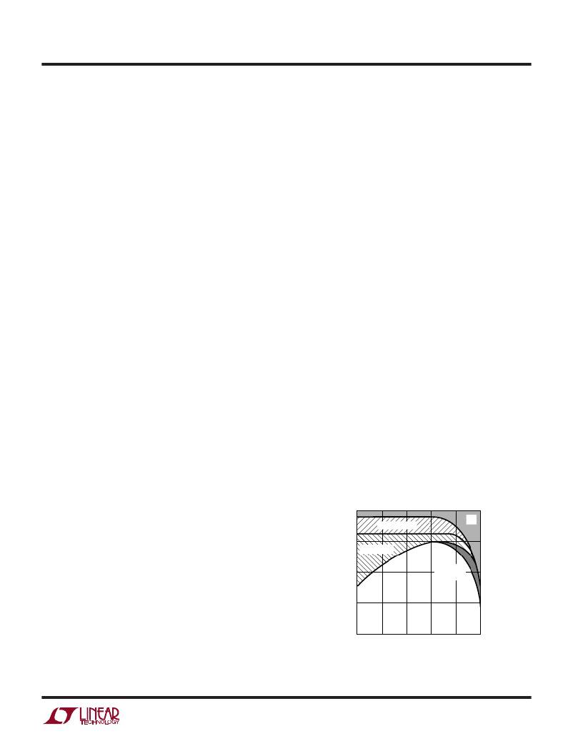
�Figure� 5� shows� how� the� efficiency� losses� in� a� typical�
�LTC1147� series� regulator� end� up� being� apportioned.�
�The� gate� charge� loss� is� responsible� for� the� majority� of�
�the� efficiency� lost� in� the� midcurrent� region.� If� Burst�
�Mode� operation� was� not� employed� at� low� currents,�
�the� gate� charge� loss� alone� would� cause� efficiency� to�
�drop� to� unacceptable� levels.� With� Burst� Mode� opera-�
�tion,� the� DC� supply� current� represents� the� lone� (and�
�unavoidable)� loss� component� which� continues� to�
�become� a� higher� percentage� as� output� current� is�
�reduced.� As� expected,� the� I� 2� R� losses� and� Schottky�
�diode� loss� dominate� at� high� load� currents.�
�100kHz� continuous� operation� for� a� 2%� to� 3%� typical�
�midcurrent� loss� with� V� IN� =� 10V.�
�Note� that� the� gate� charge� loss� increases� directly� with�
�both� input� voltage� and� operating� frequency.� This� is� the�
�principal� reason� why� the� highest� efficiency� circuits�
�operate� at� moderate� frequencies.� Furthermore,� it� ar-�
�gues� against� using� a� larger� MOSFET� than� necessary� to�
�control� I� 2� R� losses,� since� overkill� can� cost� efficiency� as�
�100�
�95�
�90�
�85�
�GATE CHARGE�
�LTC1147� I� Q�
�SCHOTTKY�
�DIODE�
�I� 2� R�
�well� as� money!�
�3.� I� 2� R� losses� are� easily� predicted� from� the� DC� resis-�
�tances� of� the� MOSFET,� inductor� and� current� shunt.� In�
�continuous� mode� the� average� output� current� flows�
�80�
�0.01�
�0.03�
�0.1� 0.3�
�OUTPUT� CURRENT� (A)�
�1�
�3�
�LTC1147� ?� F05�
�through� L� and� R� SENSE� ,� but� is� “chopped”� between� the�
�Figure� 5.� Efficiency� Loss�
�sn1147� 1147fds�
�11�
�相关PDF资料 |
PDF描述 |
|---|---|
| SPD62-103M | INDUCTOR PWR SHIELDED 10.0UH SMD |
| LTC3830-1ES8#PBF | IC REG CTRLR BUCK PWM VM 8-SOIC |
| LTC3830-1ES8 | IC REG CTRLR BUCK PWM VM 8-SOIC |
| LTC3823IGN#PBF | IC REG CTRLR BUCK PWM CM 28-SSOP |
| SPD62-682M | INDUCTOR PWR SHIELDED 6.80UH SMD |
相关代理商/技术参数 |
参数描述 |
|---|---|
| LTC1147HVCS8-3.3 | 功能描述:IC REG CTRLR BUCK PWM CM 8-SOIC RoHS:否 类别:集成电路 (IC) >> PMIC - 稳压器 - DC DC 切换控制器 系列:- 标准包装:2,500 系列:- PWM 型:电流模式 输出数:1 频率 - 最大:500kHz 占空比:96% 电源电压:4 V ~ 36 V 降压:无 升压:是 回扫:无 反相:无 倍增器:无 除法器:无 Cuk:无 隔离:无 工作温度:-40°C ~ 125°C 封装/外壳:24-WQFN 裸露焊盘 包装:带卷 (TR) |
| LTC1147HVCS8-3.3#PBF | 功能描述:IC REG CTRLR BUCK PWM CM 8-SOIC RoHS:是 类别:集成电路 (IC) >> PMIC - 稳压器 - DC DC 切换控制器 系列:- 标准包装:4,000 系列:- PWM 型:电压模式 输出数:1 频率 - 最大:1.5MHz 占空比:66.7% 电源电压:4.75 V ~ 5.25 V 降压:是 升压:无 回扫:无 反相:无 倍增器:无 除法器:无 Cuk:无 隔离:无 工作温度:-40°C ~ 85°C 封装/外壳:40-VFQFN 裸露焊盘 包装:带卷 (TR) |
| LTC1147HVCS8-3.3#TR | 功能描述:IC REG CTRLR BUCK PWM CM 8-SOIC RoHS:否 类别:集成电路 (IC) >> PMIC - 稳压器 - DC DC 切换控制器 系列:- 标准包装:2,500 系列:- PWM 型:电流模式 输出数:1 频率 - 最大:500kHz 占空比:96% 电源电压:4 V ~ 36 V 降压:无 升压:是 回扫:无 反相:无 倍增器:无 除法器:无 Cuk:无 隔离:无 工作温度:-40°C ~ 125°C 封装/外壳:24-WQFN 裸露焊盘 包装:带卷 (TR) |
| LTC1147HVCS8-3.3#TRPBF | 功能描述:IC REG CTRLR BUCK PWM CM 8-SOIC RoHS:是 类别:集成电路 (IC) >> PMIC - 稳压器 - DC DC 切换控制器 系列:- 标准包装:4,000 系列:- PWM 型:电压模式 输出数:1 频率 - 最大:1.5MHz 占空比:66.7% 电源电压:4.75 V ~ 5.25 V 降压:是 升压:无 回扫:无 反相:无 倍增器:无 除法器:无 Cuk:无 隔离:无 工作温度:-40°C ~ 85°C 封装/外壳:40-VFQFN 裸露焊盘 包装:带卷 (TR) |
| LTC1147I | 制造商:LINER 制造商全称:Linear Technology 功能描述:High Efficiency Step-Down Switching Regulator Controllers |
发布紧急采购,3分钟左右您将得到回复。