- 您现在的位置:买卖IC网 > PDF目录15286 > LTC1148CS (Linear Technology)IC REG CTRLR BUCK PWM CM 14-SOIC PDF资料下载
参数资料
| 型号: | LTC1148CS |
| 厂商: | Linear Technology |
| 文件页数: | 11/20页 |
| 文件大小: | 0K |
| 描述: | IC REG CTRLR BUCK PWM CM 14-SOIC |
| 标准包装: | 55 |
| PWM 型: | 电流模式 |
| 输出数: | 1 |
| 频率 - 最大: | 250kHz |
| 占空比: | 100% |
| 电源电压: | 3.5 V ~ 18 V |
| 降压: | 是 |
| 升压: | 无 |
| 回扫: | 无 |
| 反相: | 无 |
| 倍增器: | 无 |
| 除法器: | 无 |
| Cuk: | 无 |
| 隔离: | 无 |
| 工作温度: | 0°C ~ 70°C |
| 封装/外壳: | 14-SOIC(0.154",3.90mm 宽) |
| 包装: | 管件 |
�� �
�
�LTC1148�
�LTC1148-3.3/LTC1148-5�
�APPLICATIO� S� I� FOR� ATIO�
�In� surface� mount� applications� multiple� capacitors� may�
�have� to� be� paralleled� to� meet� the� capacitance,� ESR,� or�
�RMS� current� handling� requirements� of� the� application.�
�Aluminum� electrolytic� and� dry� tantalum� capacitors� are�
�both� available� in� surface� mount� configurations.� In� the�
�case� of� tantalum,� it� is� critical� that� the� capacitors� are� surge�
�tested� for� use� in� switching� power� supplies.� An� excellent�
�choice� is� the� AVX� TPS� series� of� surface� mount� tantalums,�
�available� in� case� heights� ranging� from� 2mm� to� 4mm.� For�
�example,� if� 200� μ� F/10V� is� called� for� in� an� application�
�requiring� 3mm� height,� two� AVX� 100� μ� F/10V� (P/N� TPSD�
�107K010)� could� be� used.� Consult� the� manufacturer� for�
�other� specific� recommendations.�
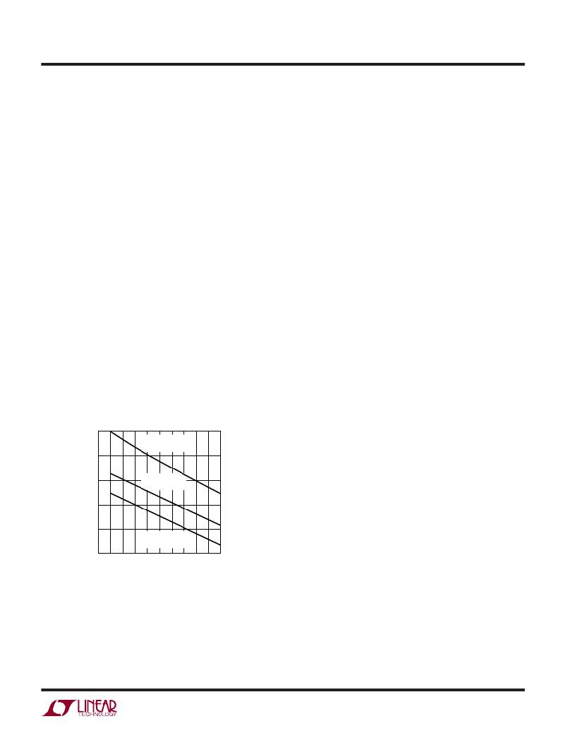
�At� low� supply� voltages,� a� minimum� capacitance� at� C� OUT�
�is� needed� to� prevent� an� abnormal� low� frequency� oper-�
�ating� mode� (see� Figure� 4).� When� C� OUT� is� made� too�
�small,� the� output� ripple� at� low� frequencies� will� be� large�
�enough� to� trip� the� voltage� comparator.� This� causes�
�Burst� Mode� operation� to� be� activated� when� the� LTC1148�
�series� would� normally� be� in� continuous� operation.� The�
�effect� is� most� pronounced� with� low� values� of� R� SENSE�
�and� can� be� improved� by� operating� at� higher� frequencies�
�with� lower� values� of� L.� The� output� remains� in� regulation�
�at� all� times.�
�1000�
�several� cycles� to� respond� to� a� step� in� DC� (resistive)� load�
�current.� When� a� load� step� occurs,� V� OUT� shifts� by� an�
�amount� equal� to� ?� I� LOAD� ?� ESR,� where� ESR� is� the� effective�
�series� resistance� of� C� OUT� .� ?� I� LOAD� also� begins� to� charge�
�or� discharge� C� OUT� until� the� regulator� loop� adapts� to� the�
�current� change� and� returns� V� OUT� to� its� steady� state�
�value.� During� this� recovery� time� V� OUT� can� be� monitored�
�for� overshoot� or� ringing� which� would� indicate� a� stability�
�problem.� The� Pin� 6� external� components� shown� in� the�
�Figure� 1� circuit� will� prove� adequate� compensation� for�
�most� applications.�
�A� second,� more� severe� transient� is� caused� by� switching� in�
�loads� with� large� (>1� μ� F)� supply� bypass� capacitors.� The�
�discharged� bypass� capacitors� are� effectively� put� in� parallel�
�with� C� OUT� ,� causing� a� rapid� drop� in� V� OUT� .� No� regulator� can�
�deliver� enough� current� to� prevent� this� problem� if� the� load�
�switch� resistance� is� low� and� it� is� driven� quickly.� The� only�
�solution� is� to� limit� the� rise� time� of� the� switch� drive� so� that�
�the� load� rise� time� is� limited� to� approximately� 25� ?� C� LOAD� .�
�Thus� a� 10� μ� F� capacitor� would� require� a� 250� μ� s� rise� time,�
�limiting� the� charging� current� to� about� 200mA.�
�Efficiency� Considerations�
�The� percent� efficiency� of� a� switching� regulator� is� equal� to�
�the� output� power� divided� by� the� input� power� times� 100%.�
�800�
�600�
�400�
�200�
�L� =� 50� μ� H�
�R� SENSE� =� 0.02� ?�
�L� =� 25� μ� H�
�R� SENSE� =� 0.02� ?�
�L� =� 50� μ� H�
�R� SENSE� =� 0.05� ?�
�It� is� often� useful� to� analyze� individual� losses� to� determine�
�what� is� limiting� the� efficiency� and� which� change� would�
�produce� the� most� improvement.� Percent� efficiency� can� be�
�expressed� as:�
�%Efficiency� =� 100%� –� (L1� +� L2� +� L3� +� ...)�
�where� L1,� L2,� etc.,� are� the� individual� losses� as� a� percent-�
�age� of� input� power.� (For� high� efficiency� circuits� only� small�
�errors� are� incurred� by� expressing� losses� as� a� percentage�
�0�
�0�
�1�
�2�
�3�
�4�
�5�
�of� output� power).�
�(V� IN� –� V� OUT� )� VOLTAGE� (V)�
�LTC1148� ?� F04�
�Although� all� dissipative� elements� in� the� circuit� produce�
�losses,� three� main� sources� usually� account� for� most� of� the�
�Figure� 4.� Minimum� Value� of� C� OUT�
�Checking� Transient� Response�
�The� regulator� loop� response� can� be� checked� by� looking�
�at� the� load� transient� response.� Switching� regulators� take�
�losses� in� LTC1148� series� circuits:� 1)� LTC1148� DC� bias�
�current,� 2)� MOSFET� gate� charge� current,� and� 3)� I� 2� R�
�losses.�
�1.� The� DC� supply� current� is� the� current� which� flows� into�
�V� IN� Pin� 3� less� the� gate� charge� current.� For� V� IN� =� 10V� the�
�114835fd�
�11�
�相关PDF资料 |
PDF描述 |
|---|---|
| VI-B2Z-EY-F1 | CONVERTER MOD DC/DC 2V 20W |
| LTC1148CS-5 | IC REG CTRLR BUCK PWM CM 14-SOIC |
| VI-B2Z-EX-F4 | CONVERTER MOD DC/DC 2V 30W |
| LTC1148CS-3.3#PBF | IC REG CTRLR BUCK PWM CM 14-SOIC |
| VI-B2Z-EX-F3 | CONVERTER MOD DC/DC 2V 30W |
相关代理商/技术参数 |
参数描述 |
|---|---|
| LTC1148CS#PBF | 功能描述:IC REG CTRLR BUCK PWM CM 14-SOIC RoHS:是 类别:集成电路 (IC) >> PMIC - 稳压器 - DC DC 切换控制器 系列:- 特色产品:LM3753/54 Scalable 2-Phase Synchronous Buck Controllers 标准包装:1 系列:PowerWise® PWM 型:电压模式 输出数:1 频率 - 最大:1MHz 占空比:81% 电源电压:4.5 V ~ 18 V 降压:是 升压:无 回扫:无 反相:无 倍增器:无 除法器:无 Cuk:无 隔离:无 工作温度:-5°C ~ 125°C 封装/外壳:32-WFQFN 裸露焊盘 包装:Digi-Reel® 产品目录页面:1303 (CN2011-ZH PDF) 其它名称:LM3754SQDKR |
| LTC1148CS#TR | 功能描述:IC REG CTRLR BUCK PWM CM 14-SOIC RoHS:否 类别:集成电路 (IC) >> PMIC - 稳压器 - DC DC 切换控制器 系列:- 标准包装:4,500 系列:PowerWise® PWM 型:控制器 输出数:1 频率 - 最大:1MHz 占空比:95% 电源电压:2.8 V ~ 5.5 V 降压:是 升压:无 回扫:无 反相:无 倍增器:无 除法器:无 Cuk:无 隔离:无 工作温度:-40°C ~ 125°C 封装/外壳:6-WDFN 裸露焊盘 包装:带卷 (TR) 配用:LM1771EVAL-ND - BOARD EVALUATION LM1771 其它名称:LM1771SSDX |
| LTC1148CS#TRPBF | 功能描述:IC REG CTRLR BUCK PWM CM 14-SOIC RoHS:是 类别:集成电路 (IC) >> PMIC - 稳压器 - DC DC 切换控制器 系列:- 标准包装:4,500 系列:PowerWise® PWM 型:控制器 输出数:1 频率 - 最大:1MHz 占空比:95% 电源电压:2.8 V ~ 5.5 V 降压:是 升压:无 回扫:无 反相:无 倍增器:无 除法器:无 Cuk:无 隔离:无 工作温度:-40°C ~ 125°C 封装/外壳:6-WDFN 裸露焊盘 包装:带卷 (TR) 配用:LM1771EVAL-ND - BOARD EVALUATION LM1771 其它名称:LM1771SSDX |
| LTC1148CS-3.3 | 功能描述:IC REG CTRLR BUCK PWM CM 14-SOIC RoHS:否 类别:集成电路 (IC) >> PMIC - 稳压器 - DC DC 切换控制器 系列:- 标准包装:4,500 系列:PowerWise® PWM 型:控制器 输出数:1 频率 - 最大:1MHz 占空比:95% 电源电压:2.8 V ~ 5.5 V 降压:是 升压:无 回扫:无 反相:无 倍增器:无 除法器:无 Cuk:无 隔离:无 工作温度:-40°C ~ 125°C 封装/外壳:6-WDFN 裸露焊盘 包装:带卷 (TR) 配用:LM1771EVAL-ND - BOARD EVALUATION LM1771 其它名称:LM1771SSDX |
| LTC1148CS-3.3#PBF | 功能描述:IC REG CTRLR BUCK PWM CM 14-SOIC RoHS:是 类别:集成电路 (IC) >> PMIC - 稳压器 - DC DC 切换控制器 系列:- 标准包装:4,500 系列:PowerWise® PWM 型:控制器 输出数:1 频率 - 最大:1MHz 占空比:95% 电源电压:2.8 V ~ 5.5 V 降压:是 升压:无 回扫:无 反相:无 倍增器:无 除法器:无 Cuk:无 隔离:无 工作温度:-40°C ~ 125°C 封装/外壳:6-WDFN 裸露焊盘 包装:带卷 (TR) 配用:LM1771EVAL-ND - BOARD EVALUATION LM1771 其它名称:LM1771SSDX |
发布紧急采购,3分钟左右您将得到回复。