- 您现在的位置:买卖IC网 > PDF目录15286 > LTC1148CS (Linear Technology)IC REG CTRLR BUCK PWM CM 14-SOIC PDF资料下载
参数资料
| 型号: | LTC1148CS |
| 厂商: | Linear Technology |
| 文件页数: | 12/20页 |
| 文件大小: | 0K |
| 描述: | IC REG CTRLR BUCK PWM CM 14-SOIC |
| 标准包装: | 55 |
| PWM 型: | 电流模式 |
| 输出数: | 1 |
| 频率 - 最大: | 250kHz |
| 占空比: | 100% |
| 电源电压: | 3.5 V ~ 18 V |
| 降压: | 是 |
| 升压: | 无 |
| 回扫: | 无 |
| 反相: | 无 |
| 倍增器: | 无 |
| 除法器: | 无 |
| Cuk: | 无 |
| 隔离: | 无 |
| 工作温度: | 0°C ~ 70°C |
| 封装/外壳: | 14-SOIC(0.154",3.90mm 宽) |
| 包装: | 管件 |
�� �
�
�LTC1148�
�LTC1148-3.3/LTC1148-5�
�APPLICATIO� S� I� FOR� ATIO�
�LTC1148� DC� supply� current� is� 160� μ� A� for� no� load,� and�
�increases� proportionally� with� load� up� to� a� constant�
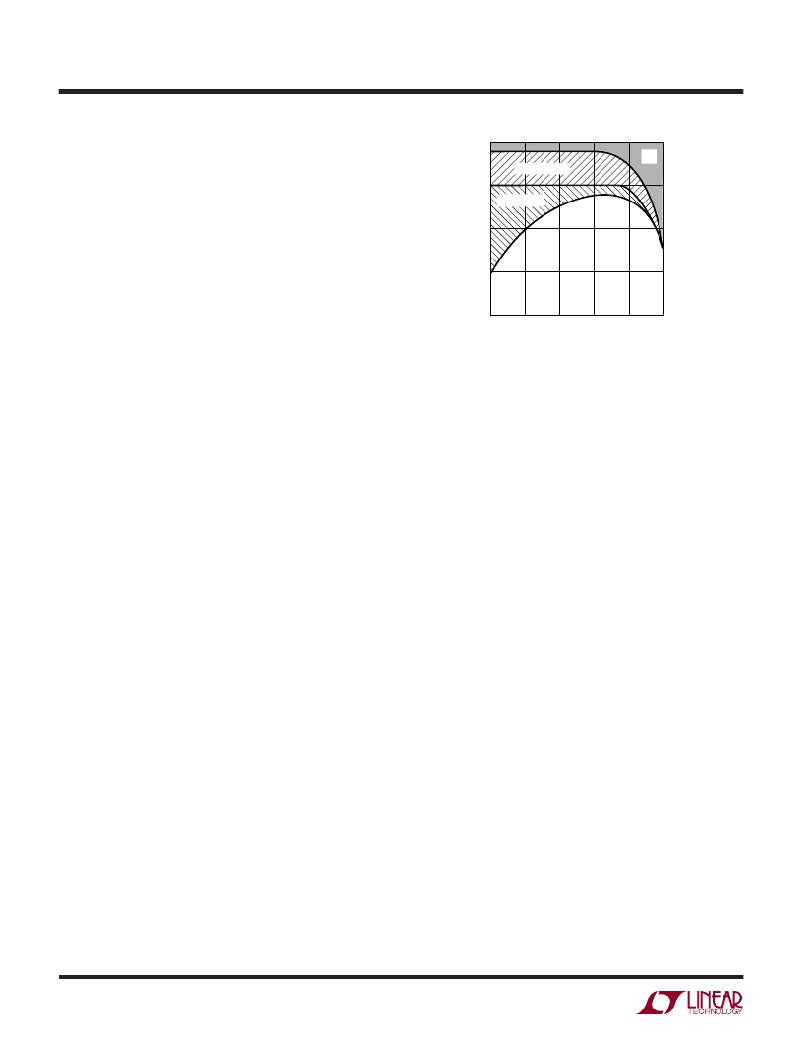
�100�
�GATE CHARGE�
�I� 2� R�
�1.6mA� after� the� LTC1148� series� has� entered� continu-�
�ous� mode.� Because� the� DC� bias� current� is� drawn� from�
�V� IN� ,� the� resulting� loss� increases� with� input� voltage.� For�
�V� IN� =� 10V� the� DC� bias� losses� are� generally� less� than� 1%�
�for� load� currents� over� 30mA.� However,� at� very� low� load�
�currents� the� DC� bias� current� accounts� for� nearly� all� of�
�the� loss.�
�95�
�90�
�85�
�LTC1148� I� Q�
�2.� MOSFET� gate� charge� current� results� from� switching� the�
�80�
�0.01�
�0.03�
�0.1�
�0.3�
�1�
�3�
�gate� capacitance� of� the� power� MOSFETs.� Each� time� a�
�MOSFET� gate� is� switched� from� low� to� high� to� low� again,�
�a� packet� of� charge� dQ� moves� from� V� IN� to� ground.� The�
�resulting� dQ/dt� is� a� current� out� of� V� IN� which� is� typically�
�much� larger� than� the� DC� supply� current.� In� continuous�
�mode,� I� GATECHG� =� f� (Q� N� +� Q� P� ).� The� typical� gate� charge�
�for� a� 0.1� ?� N-channel� power� MOSFET� is� 25nC,� and� for�
�a� P-channel� about� twice� that� value.� This� results� in�
�I� GATECHG� =� 7.5mA� in� 100kHz� continuous� operation,� for�
�a� 2%� to� 3%� typical� mid-current� loss� with� V� IN� =� 10V.�
�Note� that� the� gate� charge� loss� increases� directly� with�
�both� input� voltage� and� operating� frequency.� This� is� the�
�principal� reason� why� the� highest� efficiency� circuits�
�operate� at� moderate� frequencies.� Furthermore,� it� ar-�
�gues� against� using� larger� MOSFETs� than� necessary� to�
�control� I� 2� R� losses,� since� overkill� can� cost� efficiency� as�
�well� as� money!�
�3.� I� 2� R� losses� are� easily� predicted� from� the� DC� resistances�
�of� the� MOSFET,� inductor,� and� current� shunt.� In� continu-�
�ous� mode� the� average� output� current� flows� through� L�
�and� R� SENSE� ,� but� is� “chopped”� between� the� P-channel�
�and� N-channel� MOSFETs.� If� the� two� MOSFETs� have�
�approximately� the� same� R� DS(ON)� ,� then� the� resistance� of�
�one� MOSFET� can� simply� be� summed� with� the� resis-�
�tances� of� L� and� R� SENSE� to� obtain� I� 2� R� losses.� For�
�example,� if� each� R� DS(ON)� =� 0.1� ?� ,� R� L� =� 0.15� ?� ,� and�
�R� SENSE� =� 0.05� ?� ,� then� the� total� resistance� is� 0.3� ?� .� This�
�results� in� losses� ranging� from� 3%� to� 12%� as� the� output�
�current� increases� from� 0.5A� to� 2A.� I� 2� R� losses� cause� the�
�efficiency� to� roll-off� at� high� output� currents.�
�Figure� 5� shows� how� the� efficiency� losses� in� a� typical�
�LTC1148� series� regulator� end� up� being� apportioned.�
�OUTPUT� CURRENT� (A)�
�LTC1148� ?� F05�
�Figure� 5.� Efficiency� Loss�
�The� gate� charge� loss� is� responsible� for� the� majority� of�
�the� efficiency� lost� in� the� mid-current� region.� If� Burst�
�Mode� operation� was� not� employed� at� low� currents,� the�
�gate� charge� loss� alone� would� cause� efficiency� to� drop� to�
�unacceptable� levels.� With� Burst� Mode� operation,� the�
�DC� supply� current� represents� the� lone� (and� unavoid-�
�able)� loss� component� which� continues� to� become� a�
�higher� percentage� as� output� current� is� reduced.� As�
�expected,� the� I� 2� R� losses� dominate� at� high� load� currents.�
�Other� losses� including� C� IN� and� C� OUT� ESR� dissipative�
�losses,� MOSFET� switching� losses,� Schottky� conduction�
�losses� during� dead� time,� and� inductor� core� losses,� gener-�
�ally� account� for� less� than� 2%� total� additional� loss.�
�Design� Example�
�As� a� design� example,� assume� V� IN� =� 12V� (nominal),�
�V� OUT� =� 5V,� I� MAX� =� 2A,� and� f� =� 200kHz;� R� SENSE� ,� C� T� and� L�
�can� immediately� be� calculated:�
�R� SENSE� =� 100mV/2� =� 0.05� ?�
�t� OFF� =� (1/200kHz)[1� –� (5/12)]� =� 2.92� μ� s�
�C� T� =� 2.92� μ� s/[(1.3)(10� 4� )]� =� 220pF�
�L� MIN� =� 5.1(10� 5� )0.05� ?� (220pF)5V� =� 28� μ� H�
�Assume� that� the� MOSFET� dissipations� are� to� be� limited� to�
�P� N� =� P� P� =� 250mW.�
�If� T� A� =� 50� °� C� and� the� thermal� resistance� of� each� MOSFET�
�is� 50� °� C/� W,� then� the� junction� temperatures� will� be� 63� °� C�
�114835fd�
�12�
�相关PDF资料 |
PDF描述 |
|---|---|
| VI-B2Z-EY-F1 | CONVERTER MOD DC/DC 2V 20W |
| LTC1148CS-5 | IC REG CTRLR BUCK PWM CM 14-SOIC |
| VI-B2Z-EX-F4 | CONVERTER MOD DC/DC 2V 30W |
| LTC1148CS-3.3#PBF | IC REG CTRLR BUCK PWM CM 14-SOIC |
| VI-B2Z-EX-F3 | CONVERTER MOD DC/DC 2V 30W |
相关代理商/技术参数 |
参数描述 |
|---|---|
| LTC1148CS#PBF | 功能描述:IC REG CTRLR BUCK PWM CM 14-SOIC RoHS:是 类别:集成电路 (IC) >> PMIC - 稳压器 - DC DC 切换控制器 系列:- 特色产品:LM3753/54 Scalable 2-Phase Synchronous Buck Controllers 标准包装:1 系列:PowerWise® PWM 型:电压模式 输出数:1 频率 - 最大:1MHz 占空比:81% 电源电压:4.5 V ~ 18 V 降压:是 升压:无 回扫:无 反相:无 倍增器:无 除法器:无 Cuk:无 隔离:无 工作温度:-5°C ~ 125°C 封装/外壳:32-WFQFN 裸露焊盘 包装:Digi-Reel® 产品目录页面:1303 (CN2011-ZH PDF) 其它名称:LM3754SQDKR |
| LTC1148CS#TR | 功能描述:IC REG CTRLR BUCK PWM CM 14-SOIC RoHS:否 类别:集成电路 (IC) >> PMIC - 稳压器 - DC DC 切换控制器 系列:- 标准包装:4,500 系列:PowerWise® PWM 型:控制器 输出数:1 频率 - 最大:1MHz 占空比:95% 电源电压:2.8 V ~ 5.5 V 降压:是 升压:无 回扫:无 反相:无 倍增器:无 除法器:无 Cuk:无 隔离:无 工作温度:-40°C ~ 125°C 封装/外壳:6-WDFN 裸露焊盘 包装:带卷 (TR) 配用:LM1771EVAL-ND - BOARD EVALUATION LM1771 其它名称:LM1771SSDX |
| LTC1148CS#TRPBF | 功能描述:IC REG CTRLR BUCK PWM CM 14-SOIC RoHS:是 类别:集成电路 (IC) >> PMIC - 稳压器 - DC DC 切换控制器 系列:- 标准包装:4,500 系列:PowerWise® PWM 型:控制器 输出数:1 频率 - 最大:1MHz 占空比:95% 电源电压:2.8 V ~ 5.5 V 降压:是 升压:无 回扫:无 反相:无 倍增器:无 除法器:无 Cuk:无 隔离:无 工作温度:-40°C ~ 125°C 封装/外壳:6-WDFN 裸露焊盘 包装:带卷 (TR) 配用:LM1771EVAL-ND - BOARD EVALUATION LM1771 其它名称:LM1771SSDX |
| LTC1148CS-3.3 | 功能描述:IC REG CTRLR BUCK PWM CM 14-SOIC RoHS:否 类别:集成电路 (IC) >> PMIC - 稳压器 - DC DC 切换控制器 系列:- 标准包装:4,500 系列:PowerWise® PWM 型:控制器 输出数:1 频率 - 最大:1MHz 占空比:95% 电源电压:2.8 V ~ 5.5 V 降压:是 升压:无 回扫:无 反相:无 倍增器:无 除法器:无 Cuk:无 隔离:无 工作温度:-40°C ~ 125°C 封装/外壳:6-WDFN 裸露焊盘 包装:带卷 (TR) 配用:LM1771EVAL-ND - BOARD EVALUATION LM1771 其它名称:LM1771SSDX |
| LTC1148CS-3.3#PBF | 功能描述:IC REG CTRLR BUCK PWM CM 14-SOIC RoHS:是 类别:集成电路 (IC) >> PMIC - 稳压器 - DC DC 切换控制器 系列:- 标准包装:4,500 系列:PowerWise® PWM 型:控制器 输出数:1 频率 - 最大:1MHz 占空比:95% 电源电压:2.8 V ~ 5.5 V 降压:是 升压:无 回扫:无 反相:无 倍增器:无 除法器:无 Cuk:无 隔离:无 工作温度:-40°C ~ 125°C 封装/外壳:6-WDFN 裸露焊盘 包装:带卷 (TR) 配用:LM1771EVAL-ND - BOARD EVALUATION LM1771 其它名称:LM1771SSDX |
发布紧急采购,3分钟左右您将得到回复。