- 您现在的位置:买卖IC网 > PDF目录10348 > LTC1198-2BCS8 (Linear Technology)IC ADC 8BIT 750KHZ SAMPL 8-SOIC PDF资料下载
参数资料
| 型号: | LTC1198-2BCS8 |
| 厂商: | Linear Technology |
| 文件页数: | 3/28页 |
| 文件大小: | 0K |
| 描述: | IC ADC 8BIT 750KHZ SAMPL 8-SOIC |
| 标准包装: | 100 |
| 位数: | 8 |
| 采样率(每秒): | 750k |
| 数据接口: | 串行 |
| 转换器数目: | 1 |
| 功率耗散(最大): | 50mW |
| 电压电源: | 单电源 |
| 工作温度: | 0°C ~ 70°C |
| 安装类型: | 表面贴装 |
| 封装/外壳: | 8-SOIC(0.154",3.90mm 宽) |
| 供应商设备封装: | 8-SOIC |
| 包装: | 管件 |
| 输入数目和类型: | 1 个单端,单极 |
第1页第2页当前第3页第4页第5页第6页第7页第8页第9页第10页第11页第12页第13页第14页第15页第16页第17页第18页第19页第20页第21页第22页第23页第24页第25页第26页第27页第28页
LTC1196/LTC1198
11
119698fb
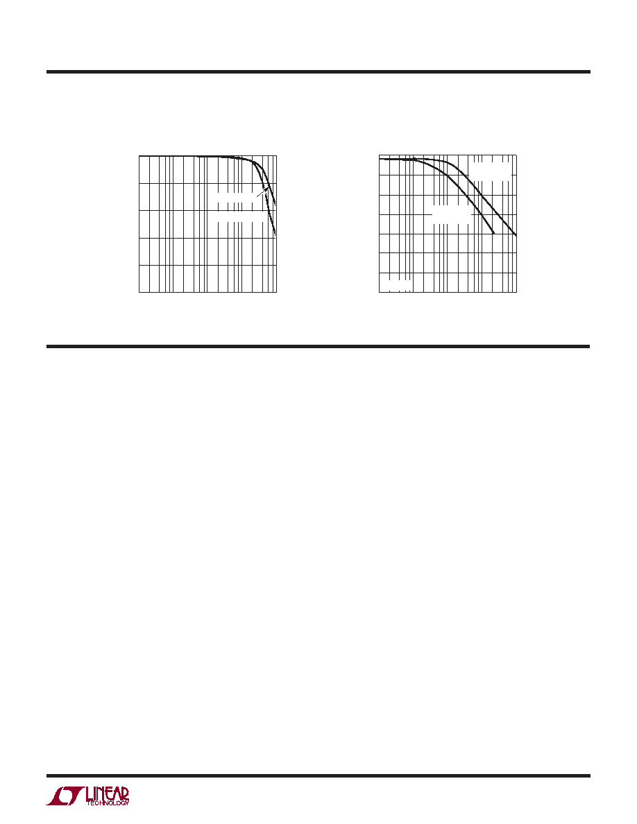
TYPICAL PERFORMANCE CHARACTERISTICS
Spurious-Free Dynamic Range
vs Frequency
Output Amplitude
vs Input Frequency
INPUT FREQUENCY (Hz)
1k
PEAK-TO-PEAK
OUTPUT
(%)
10M
1196/98 G34
10k
100k
1M
100
80
60
40
20
0
VREF = VCC = 2.7V
VREF = VCC = 5V
FREQUENCY (Hz)
1k
70
60
50
40
30
20
10
0
1M
1196/98 G35
10k
100k
10M
SPURIOUS-FREE
DYNAMIC
RANGE
(dB)
TA = 25°C
VCC = 3V
fCLK = 5MHz
VCC = 5V
fCLK = 12MHz
PIN FUNCTIONS
LTC1196
CS (Pin 1): Chip Select Input. A logic LOW on this input
enables the LTC1196. A logic HIGH on this input disables
the LTC1196.
IN+ (Pin 2): Analog Input. This input must be free of noise
with respect to GND.
IN– (Pin 3): Analog Input. This input must be free of noise
with respect to GND.
GND (Pin 4): Analog Ground. GND should be tied directly
to an analog ground plane.
VREF (Pin 5): Reference Input. The reference input denes
the span of the A/D converter and must be kept free of
noise with respect to GND.
DOUT (Pin 6): Digital Data Output. The A/D conversion
result is shifted out of this output.
CLK (Pin 7): Shift Clock. This clock synchronizes the se-
rial data transfer.
VCC(Pin8):PowerSupplyVoltage.Thispinprovidespower
to the A/D converter. It must be kept free of noise and ripple
by bypassing directly to the analog ground plane.
LTC1198
CS/SHUTDOWN (Pin 1): Chip Select Input. A logic LOW
on this input enables the LTC1198. A logic HIGH on this
input disables the LTC1198 and disconnects the power
to THE LTC1198.
CHO (Pin 2): Analog Input. This input must be free of
noise with respect to GND.
CH1 (Pin 3): Analog Input. This input must be free of noise
with respect to GND.
GND (Pin 4): Analog Ground. GND should be tied directly
to an analog ground plane.
DIN (Pin 5): Digital Data Input. The multiplexer address is
shifted into this input.
DOUT (Pin 6): Digital Data Output. The A/D conversion
result is shifted out of this output.
CLK (Pin 7): Shift Clock. This clock synchronizes the se-
rial data transfer.
VCC (VREF) (Pin 8): Power Supply and Reference Volt-
age. This pin provides power and denes the span of the
A/D converter. It must be kept free of noise and ripple by
bypassing directly to the analog ground plane.
相关PDF资料 |
PDF描述 |
|---|---|
| VI-J33-IW-B1 | CONVERTER MOD DC/DC 24V 100W |
| VI-J3H-IW-B1 | CONVERTER MOD DC/DC 52V 100W |
| LTC2436-1IGN#TR | IC CONV A/D 16B 2CH DIFF 16SSOP |
| VI-J3D-IW-B1 | CONVERTER MOD DC/DC 85V 100W |
| D38999/20JE26AN | CONN HSG RCPT 26POS WALL MT PINS |
相关代理商/技术参数 |
参数描述 |
|---|---|
| LTC1198-2BCS8#PBF | 功能描述:IC ADC 8BIT 750KHZ SAMPL 8-SOIC RoHS:是 类别:集成电路 (IC) >> 数据采集 - 模数转换器 系列:- 其它有关文件:TSA1204 View All Specifications 标准包装:1 系列:- 位数:12 采样率(每秒):20M 数据接口:并联 转换器数目:2 功率耗散(最大):155mW 电压电源:模拟和数字 工作温度:-40°C ~ 85°C 安装类型:表面贴装 封装/外壳:48-TQFP 供应商设备封装:48-TQFP(7x7) 包装:Digi-Reel® 输入数目和类型:4 个单端,单极;2 个差分,单极 产品目录页面:1156 (CN2011-ZH PDF) 其它名称:497-5435-6 |
| LTC1198-2BCS8#TR | 功能描述:IC ADC 8BIT 750KHZ SHUTDWN 8SOIC RoHS:否 类别:集成电路 (IC) >> 数据采集 - 模数转换器 系列:- 标准包装:2,500 系列:- 位数:16 采样率(每秒):15 数据接口:MICROWIRE?,串行,SPI? 转换器数目:1 功率耗散(最大):480µW 电压电源:单电源 工作温度:-40°C ~ 85°C 安装类型:表面贴装 封装/外壳:38-WFQFN 裸露焊盘 供应商设备封装:38-QFN(5x7) 包装:带卷 (TR) 输入数目和类型:16 个单端,双极;8 个差分,双极 配用:DC1011A-C-ND - BOARD DELTA SIGMA ADC LTC2494 |
| LTC1198-2BCS8#TRPBF | 功能描述:IC ADC 8BIT 750KHZ SAMPL 8-SOIC RoHS:是 类别:集成电路 (IC) >> 数据采集 - 模数转换器 系列:- 标准包装:2,500 系列:- 位数:16 采样率(每秒):15 数据接口:MICROWIRE?,串行,SPI? 转换器数目:1 功率耗散(最大):480µW 电压电源:单电源 工作温度:-40°C ~ 85°C 安装类型:表面贴装 封装/外壳:38-WFQFN 裸露焊盘 供应商设备封装:38-QFN(5x7) 包装:带卷 (TR) 输入数目和类型:16 个单端,双极;8 个差分,双极 配用:DC1011A-C-ND - BOARD DELTA SIGMA ADC LTC2494 |
| LTC1198-2BCS8-PBF | 制造商:LINER 制造商全称:Linear Technology 功能描述:8-Bit, SO-8, 1Msps ADCs with Auto-Shutdown Options |
| LTC1198-2BCS8-TRPBF | 制造商:LINER 制造商全称:Linear Technology 功能描述:8-Bit, SO-8, 1Msps ADCs with Auto-Shutdown Options |
发布紧急采购,3分钟左右您将得到回复。