- 您现在的位置:买卖IC网 > PDF目录10348 > LTC1198-2BCS8 (Linear Technology)IC ADC 8BIT 750KHZ SAMPL 8-SOIC PDF资料下载
参数资料
| 型号: | LTC1198-2BCS8 |
| 厂商: | Linear Technology |
| 文件页数: | 7/28页 |
| 文件大小: | 0K |
| 描述: | IC ADC 8BIT 750KHZ SAMPL 8-SOIC |
| 标准包装: | 100 |
| 位数: | 8 |
| 采样率(每秒): | 750k |
| 数据接口: | 串行 |
| 转换器数目: | 1 |
| 功率耗散(最大): | 50mW |
| 电压电源: | 单电源 |
| 工作温度: | 0°C ~ 70°C |
| 安装类型: | 表面贴装 |
| 封装/外壳: | 8-SOIC(0.154",3.90mm 宽) |
| 供应商设备封装: | 8-SOIC |
| 包装: | 管件 |
| 输入数目和类型: | 1 个单端,单极 |
第1页第2页第3页第4页第5页第6页当前第7页第8页第9页第10页第11页第12页第13页第14页第15页第16页第17页第18页第19页第20页第21页第22页第23页第24页第25页第26页第27页第28页
LTC1196/LTC1198
15
119698fb
APPLICATIONS INFORMATION
Connection to a microprocessor or a DSP serial port is
quite simple (see the Data Transfer section). It requires no
additional hardware, but the speed will be limited by the
clock rate of the microprocessor or the DSP which limits
the conversion time of the LTC1196/LTC1198.
Data Transfer
Data transfer differs slightly between the LTC1196 and
the LTC1198. The LTC1196 interfaces over three lines:
CS, CLK and DOUT. A falling CS initiates data transfer as
depicted by the LTC1196 Operating Sequence in Figure 1.
After CS falls, the rst CLK pulse enables DOUT. After two
null bits, the A/D conversion result is output on the DOUT
line. Bringing CS HIGH resets the LTC1196 for the next
data exchange.
The LTC1198 can transfer data with three or four wires.
The additional input, DIN, is used to select the 2-channel
MUX conguration.
The data transfer between the LTC1198 and the digital
systems can be broken into two sections: Input Data
Word and A/D Conversion Result. First, each bit of the
input data word is captured on the rising CLK edge by the
LTC1198. Second, each bit of the A/D conversion result
on the DOUT line is updated on the rising CLK edge by the
LTC1198. This bit should be captured on the next rising
CLK edge by the digital systems (see the A/D Conversion
Result section).
Data transfer is initiated by a falling chip select (CS) signal
as depicted by the LTC1198 Operating Sequence in Figure 2.
After CS falls, the LTC1198 looks for a START bit. After
the START bit is received, the 4-bit input word is shifted
into the DIN input. The rst two bits of the input word
congure the LTC1198. The last two bits of the input word
allow the ADC to acquire the input voltage by 2.5 clocks
before the conversion starts. After the conversion starts,
two null bits and the conversion result are output on the
DOUT line. At the end of the data exchange CS should be
brought HIGH. This resets the LTC1198 in preparation for
the next data exchange.
Input Data Word
The LTC1196 requires no DIN word. It is permanently con-
gured to have a single differential input. The conversion
result is output on the DOUT line in an MSB-rst sequence,
followed by zeros indenitely if clocks are continuously
applied with CS LOW.
The LTC1198 clocks data into the DIN input on the ris-
ing edge of the clock. The input data word is dened as
follows:
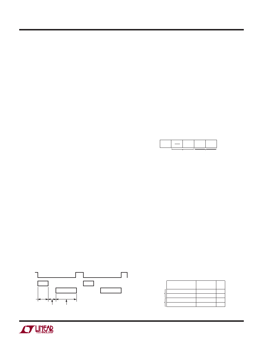
DIN1
DIN2
DOUT1
DOUT2
CS
SHIFT MUX
ADDRESS IN
2 NULL BITS
SHIFT A/D CONVERSION
RESULT OUT
1196/98 AI01
SGL/
DIFF
ODD/
SIGN
DUMMY
START
MUX
ADDRESS
DUMMY
BITS
119698 AI02
DUMMY
START Bit
The rst
logical one clocked into the DIN input after CS
goes LOW is the START bit. The START bit initiates the data
transfer. The LTC1198 will ignore all leading zeros which
precede this
logical one. After the START bit is received,
the remaining bits of the input word will be clocked in.
Further inputs on the DIN pin are then ignored until the
next CS cycle.
Multiplexer (MUX) Address
The two bits of the input word following the START bit as-
sign the MUX conguration for the requested conversion.
For a given channel selection, the converter will measure
the voltage between the two channels indicated by the “+”
and “–” signs in the selected row of the following table.
In single-ended mode, all input channels are measured
with respect to GND.
MUX ADDRESS
SGL/DIFF
1
0
ODD/SIGN
0
1
0
1
CHANNEL #
0
+
–
1
+
–
+
GND
–
SINGLE-ENDED
MUX MODE
DIFFERENTIAL
MUX MODE
1196/98 AI03
LTC1198 Channel Selection
相关PDF资料 |
PDF描述 |
|---|---|
| VI-J33-IW-B1 | CONVERTER MOD DC/DC 24V 100W |
| VI-J3H-IW-B1 | CONVERTER MOD DC/DC 52V 100W |
| LTC2436-1IGN#TR | IC CONV A/D 16B 2CH DIFF 16SSOP |
| VI-J3D-IW-B1 | CONVERTER MOD DC/DC 85V 100W |
| D38999/20JE26AN | CONN HSG RCPT 26POS WALL MT PINS |
相关代理商/技术参数 |
参数描述 |
|---|---|
| LTC1198-2BCS8#PBF | 功能描述:IC ADC 8BIT 750KHZ SAMPL 8-SOIC RoHS:是 类别:集成电路 (IC) >> 数据采集 - 模数转换器 系列:- 其它有关文件:TSA1204 View All Specifications 标准包装:1 系列:- 位数:12 采样率(每秒):20M 数据接口:并联 转换器数目:2 功率耗散(最大):155mW 电压电源:模拟和数字 工作温度:-40°C ~ 85°C 安装类型:表面贴装 封装/外壳:48-TQFP 供应商设备封装:48-TQFP(7x7) 包装:Digi-Reel® 输入数目和类型:4 个单端,单极;2 个差分,单极 产品目录页面:1156 (CN2011-ZH PDF) 其它名称:497-5435-6 |
| LTC1198-2BCS8#TR | 功能描述:IC ADC 8BIT 750KHZ SHUTDWN 8SOIC RoHS:否 类别:集成电路 (IC) >> 数据采集 - 模数转换器 系列:- 标准包装:2,500 系列:- 位数:16 采样率(每秒):15 数据接口:MICROWIRE?,串行,SPI? 转换器数目:1 功率耗散(最大):480µW 电压电源:单电源 工作温度:-40°C ~ 85°C 安装类型:表面贴装 封装/外壳:38-WFQFN 裸露焊盘 供应商设备封装:38-QFN(5x7) 包装:带卷 (TR) 输入数目和类型:16 个单端,双极;8 个差分,双极 配用:DC1011A-C-ND - BOARD DELTA SIGMA ADC LTC2494 |
| LTC1198-2BCS8#TRPBF | 功能描述:IC ADC 8BIT 750KHZ SAMPL 8-SOIC RoHS:是 类别:集成电路 (IC) >> 数据采集 - 模数转换器 系列:- 标准包装:2,500 系列:- 位数:16 采样率(每秒):15 数据接口:MICROWIRE?,串行,SPI? 转换器数目:1 功率耗散(最大):480µW 电压电源:单电源 工作温度:-40°C ~ 85°C 安装类型:表面贴装 封装/外壳:38-WFQFN 裸露焊盘 供应商设备封装:38-QFN(5x7) 包装:带卷 (TR) 输入数目和类型:16 个单端,双极;8 个差分,双极 配用:DC1011A-C-ND - BOARD DELTA SIGMA ADC LTC2494 |
| LTC1198-2BCS8-PBF | 制造商:LINER 制造商全称:Linear Technology 功能描述:8-Bit, SO-8, 1Msps ADCs with Auto-Shutdown Options |
| LTC1198-2BCS8-TRPBF | 制造商:LINER 制造商全称:Linear Technology 功能描述:8-Bit, SO-8, 1Msps ADCs with Auto-Shutdown Options |
发布紧急采购,3分钟左右您将得到回复。