- 您现在的位置:买卖IC网 > PDF目录15290 > LTC1266IS#TR (Linear Technology)IC REG CTRLR BST PWM CM 16-SOIC PDF资料下载
参数资料
| 型号: | LTC1266IS#TR |
| 厂商: | Linear Technology |
| 文件页数: | 12/20页 |
| 文件大小: | 0K |
| 描述: | IC REG CTRLR BST PWM CM 16-SOIC |
| 标准包装: | 2,500 |
| PWM 型: | 电流模式 |
| 输出数: | 1 |
| 频率 - 最大: | 400kHz |
| 占空比: | 100% |
| 电源电压: | 3.5 V ~ 18 V |
| 降压: | 是 |
| 升压: | 是 |
| 回扫: | 无 |
| 反相: | 无 |
| 倍增器: | 无 |
| 除法器: | 无 |
| Cuk: | 无 |
| 隔离: | 无 |
| 工作温度: | -40°C ~ 85°C |
| 封装/外壳: | 16-SOIC(0.154",3.90mm 宽) |
| 包装: | 带卷 (TR) |
�� �
�
�LTC1266�
�LTC1266-3.3/LTC1266-5�
�APPLICATIO� S� I� FOR� ATIO�
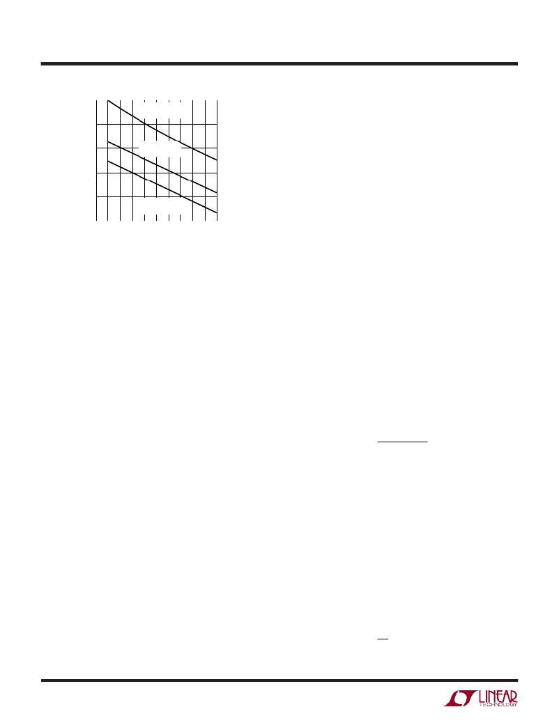
�1000�
�800�
�600�
�400�
�200�
�L� =� 50� μ� H�
�R� SENSE� =� 0.02� ?�
�L� =� 25� μ� H�
�R� SENSE� =� 0.02� ?�
�L� =� 50� μ� H�
�R� SENSE� =� 0.05� ?�
�Driving� N-Channel� Topside� MOSFETs�
�Driving� an� N-channel� topside� MOSFET� (PINV,� Pin� 3,� tied� to�
�PWR� V� IN� )� is� a� little� trickier� than� driving� a� P-channel� since�
�the� gate� voltage� must� be� positive� with� respect� to� the�
�source� to� turn� it� on,� which� means� that� the� gate� voltage�
�must� be� higher� than� V� IN� .� This� requires� either� a� second�
�supply� at� least� V� GS(ON)� above� V� IN� or� a� bootstrapping� circuit�
�to� boost� the� V� IN� to� the� proper� level.� The� easiest� method� is�
�using� a� higher� supply� (see� Figure� 14)� but� if� one� is� not�
�0�
�0�
�1�
�2�
�3�
�4�
�5�
�available,� the� bootstrap� method� can� be� used� at� the� ex-�
�(V� IN� –� V� OUT� )� VOLTAGE� (V)�
�1266� F04�
�Figure� 4.� Minimum� Value� of� C� OUT�
�series� would� normally� be� in� continuous� operation.� The�
�output� remains� in� regulation� at� all� times.� This� minimum�
�capacitance� requirement� may� be� relaxed� if� Burst� Mode�
�operation� is� disabled.�
�N-Channel� vs� P-Channel� MOSFETs�
�The� LTC1266� has� the� capability� to� drive� either� an�
�N-channel� or� a� P-channel� topside� switch� to� give� the� user�
�more� flexibility.� N-channel� MOSFETs� are� superior� in� per-�
�formance� to� P-channel� due� to� their� lower� R� DS(ON)� and�
�lower� gate� capacitance� and� are� typically� less� expensive;�
�pense� of� an� additional� diode� (see� Figure� 1).� The� bootstrap�
�works� by� charging� the� bootstrap� capacitor� to� V� IN� during�
�the� off-time.� During� the� on-time,� the� bottom� plate� of� the�
�capacitor� is� pulled� up� to� V� IN� so� that� the� voltage� at� Pin� 2� is�
�now� twice� V� IN� (plus� any� ringing� on� the� switch� node).�
�Since� the� maximum� allowable� voltage� at� Pin� 2� is� 20V,� the�
�Figure� 1� bootstrap� circuit� limits� V� IN� to� less� than� 10V.� A�
�higher� V� IN� can� be� achieved� if� the� bootstrap� capacitor� is�
�charged� to� a� voltage� less� than� V� IN� ,� in� which� case�
�V� IN(MAX)� =� 20� –� V� CAP� .�
�N-channel� mode,� internal� circuitry� limits� the� maximum�
�on-time� to� 60� μ� s� to� guarantee� start-up� of� the� bootstrap�
�circuit.� This� maximum� on-time� reduces� the� maximum�
�duty� cycle� to:�
�however,� they� do� have� a� slightly� more� complicated� gate�
�drive� requirement� and� a� more� limited� input� voltage� range�
�(see� following� sections).�
�Max� Duty� Cycle� =�
�60� μ� s�
�60� μ� s� +� t� OFF�
�)� )�
�V� TRIP� =� 1.25� 1� +� R2�
�Driving P-Channel Topside MOSFETs�
�The� P-channel� topside� switch� circuit� configuration� is� the�
�most� straightforward� due� to� the� requirement� of� only� one�
�supply� voltage� level.� This� is� due� to� the� negative� gate�
�threshold� of� the� P-channel� MOSFET� which� allows� the�
�MOSFET� to� be� switched� on� and� off� by� swinging� the� gate�
�between� V� IN� and� ground.� The� phase� invert� (Pin� 3)� is� tied�
�to� ground� to� choose� this� operating� mode.� Normally,� the�
�converter� input� (V� IN� )� is� connected� to� the� LTC1266� supply�
�Pins� 2� and� 5� and� can� go� as� high� as� 20V.� Pin� 2� supplies� the�
�high� frequency� current� pulses� to� switch� the� MOSFETs� and�
�should� be� decoupled� with� a� 0.1� μ� F� to� 1� μ� F� ceramic� capaci-�
�tor.� Pin� 5� supplies� most� of� the� quiescent� power� to� the� rest�
�of� the� chip.�
�12�
�which� slightly� increases� the� minimum� input� voltage� at�
�which� dropout� occurs.� However,� because� of� the� superior�
�on-conductance� of� the� N-channel,� the� dropout� perfor-�
�mance� of� an� all� N-channel� regulator� is� still� better� (see�
�Figure� 5)� even� with� the� duty� cycle� limitation,� except� at� light�
�loads.�
�Low-Battery� Comparator�
�The� LTC1266� has� an� on-chip� low-battery� comparator�
�which� can� be� used� to� sense� a� low-battery� condition� when�
�implemented� as� shown� in� Figure� 6.� The� resistor� divider�
�R1,� R2� sets� the� comparator� trip� point� as� follows:�
�R1�
�相关PDF资料 |
PDF描述 |
|---|---|
| LTC1266IS-5#TR | IC REG CTRLR BST PWM CM 16-SOIC |
| UPM1K331MHD6 | CAP ALUM 330UF 80V 20% RADIAL |
| LTC1735IGN-1#PBF | IC REG CTRLR BUCK PWM CM 16-SSOP |
| B41043A4687M | 680UF 16V 10X20 SINGLE END+G4400 |
| LTC1735IGN-1 | IC REG CTRLR BUCK PWM CM 16-SSOP |
相关代理商/技术参数 |
参数描述 |
|---|---|
| LTC1267CG-ADJ | 制造商:Linear Technology 功能描述:Dual High Efficiency Synchronous Step-Down Switching Regulators |
| LTC1272-3ACN | 功能描述:IC A/D CONV 12BIT SAMPLING 24DIP RoHS:否 类别:集成电路 (IC) >> 数据采集 - 模数转换器 系列:- 标准包装:1,000 系列:- 位数:12 采样率(每秒):300k 数据接口:并联 转换器数目:1 功率耗散(最大):75mW 电压电源:单电源 工作温度:0°C ~ 70°C 安装类型:表面贴装 封装/外壳:24-SOIC(0.295",7.50mm 宽) 供应商设备封装:24-SOIC 包装:带卷 (TR) 输入数目和类型:1 个单端,单极;1 个单端,双极 |
| LTC1272-3ACN#PBF | 功能描述:IC A/D CONV 12BIT SAMPLING 24DIP RoHS:是 类别:集成电路 (IC) >> 数据采集 - 模数转换器 系列:- 标准包装:1,000 系列:- 位数:12 采样率(每秒):300k 数据接口:并联 转换器数目:1 功率耗散(最大):75mW 电压电源:单电源 工作温度:0°C ~ 70°C 安装类型:表面贴装 封装/外壳:24-SOIC(0.295",7.50mm 宽) 供应商设备封装:24-SOIC 包装:带卷 (TR) 输入数目和类型:1 个单端,单极;1 个单端,双极 |
| LTC1272-3ACSW | 功能描述:IC A/D CONV 12BIT SAMPLNG 24SOIC RoHS:否 类别:集成电路 (IC) >> 数据采集 - 模数转换器 系列:- 其它有关文件:TSA1204 View All Specifications 标准包装:1 系列:- 位数:12 采样率(每秒):20M 数据接口:并联 转换器数目:2 功率耗散(最大):155mW 电压电源:模拟和数字 工作温度:-40°C ~ 85°C 安装类型:表面贴装 封装/外壳:48-TQFP 供应商设备封装:48-TQFP(7x7) 包装:Digi-Reel® 输入数目和类型:4 个单端,单极;2 个差分,单极 产品目录页面:1156 (CN2011-ZH PDF) 其它名称:497-5435-6 |
| LTC1272-3ACSW#PBF | 功能描述:IC A/D CONV 12BIT SAMPLNG 24SOIC RoHS:是 类别:集成电路 (IC) >> 数据采集 - 模数转换器 系列:- 其它有关文件:TSA1204 View All Specifications 标准包装:1 系列:- 位数:12 采样率(每秒):20M 数据接口:并联 转换器数目:2 功率耗散(最大):155mW 电压电源:模拟和数字 工作温度:-40°C ~ 85°C 安装类型:表面贴装 封装/外壳:48-TQFP 供应商设备封装:48-TQFP(7x7) 包装:Digi-Reel® 输入数目和类型:4 个单端,单极;2 个差分,单极 产品目录页面:1156 (CN2011-ZH PDF) 其它名称:497-5435-6 |
发布紧急采购,3分钟左右您将得到回复。