- 您现在的位置:买卖IC网 > PDF目录15290 > LTC1266IS#TR (Linear Technology)IC REG CTRLR BST PWM CM 16-SOIC PDF资料下载
参数资料
| 型号: | LTC1266IS#TR |
| 厂商: | Linear Technology |
| 文件页数: | 7/20页 |
| 文件大小: | 0K |
| 描述: | IC REG CTRLR BST PWM CM 16-SOIC |
| 标准包装: | 2,500 |
| PWM 型: | 电流模式 |
| 输出数: | 1 |
| 频率 - 最大: | 400kHz |
| 占空比: | 100% |
| 电源电压: | 3.5 V ~ 18 V |
| 降压: | 是 |
| 升压: | 是 |
| 回扫: | 无 |
| 反相: | 无 |
| 倍增器: | 无 |
| 除法器: | 无 |
| Cuk: | 无 |
| 隔离: | 无 |
| 工作温度: | -40°C ~ 85°C |
| 封装/外壳: | 16-SOIC(0.154",3.90mm 宽) |
| 包装: | 带卷 (TR) |
�� �
�
�LTC1266�
�LTC1266-3.3/LTC1266-5�
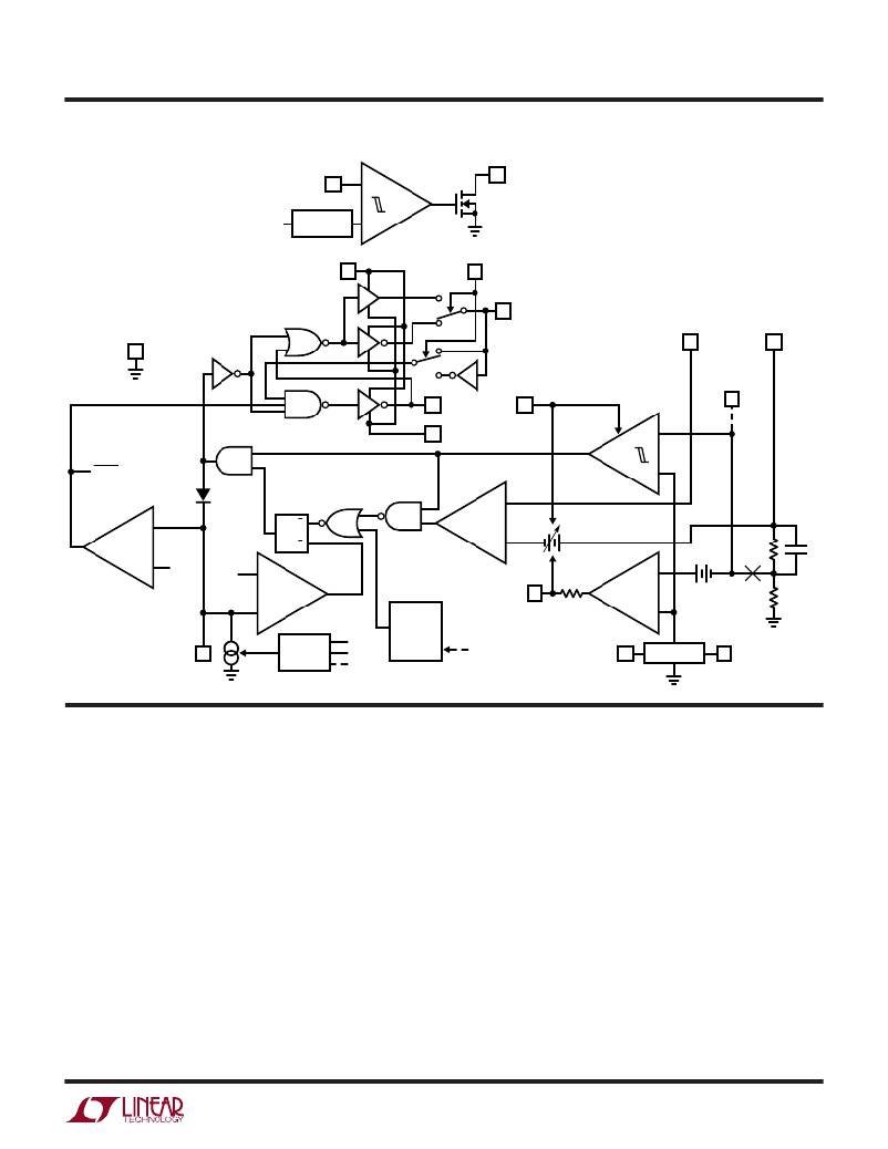
�FU� CTIO� AL� DIAGRA�
�Pin� 10� Connection� Shown� for� LTC1266-3.3� and� LTC1266-5;� Changes� Create� LTC1266�
�LB� IN� 13�
�LB�
�14� LB� OUT�
�V� IN�
�1.25V�
�REFERENCE�
�PWR� V� IN�
�2�
�3� PINV�
�1� TDRIVE�
�SIGNAL�
�GROUND�
�SENSE� +�
�9�
�SENSE� –�
�8�
�12�
�ADJUSTABLE�
�VERSION�
�V� FB�
�16� BDRIVE�
�BINH�
�4�
�10�
�15� PGND�
�V�
�SLEEP�
�S�
�+�
�–�
�V� TH2�
�V� TH1�
�Q�
�R�
�S�
�C�
�–�
�+� V� TRIP�
�13k�
�V� OS�
�5pF�
�T�
�MAX�
�ON-TIME�
�I� TH� 7�
�G�
�1.265V�
�100k�
�6�
�C� T�
�OFF-TIME�
�CONTROL�
�V� IN�
�SENSE� –�
�V� FB�
�CONTROL�
�ENABLE�
�PINV�
�SHDN� 11�
�REFERENCE�
�5� V� IN�
�1266� FD�
�OPERATIO�
�The� LTC1266� series� uses� a� current� mode,� constant� off-�
�time� architecture� to� synchronously� switch� an� external� pair�
�of� power� MOSFETs.� Operating� frequency� is� set� by� an�
�external� capacitor� at� the� timing� capacitor� Pin� 6.�
�The� output� voltage� is� sensed� by� an� internal� voltage� divider�
�connected� to� SENSE� –� ,� Pin� 8,� (LTC1266-3.3� and� LTC1266-�
�5)� or� external� divider� returned� to� V� FB� ,� Pin� 10,� (LTC1266).�
�A� voltage� comparator� V,� and� a� gain� block� G,� compare� the�
�divided� output� voltage� with� a� reference� voltage� of� 1.265V.�
�To� optimize� efficiency,� the� LTC1266� automatically� switches�
�between� two� modes� of� operation,� burst� and� continuous.�
�The� voltage� comparator� is� the� primary� control� element�
�when� the� device� is� in� Burst� Mode� operation,� while� the� gain�
�block� controls� the� output� voltage� in� continuous� mode.�
�During� the� switch� ON� cycle� in� continuous� mode,� current�
�comparator� C� monitors� the� voltage� between� Pins� 8� and� 9�
�connected� across� an� external� shunt� in� series� with� the�
�inductor.� When� the� voltage� across� the� shunt� reaches� its�
�threshold� value,� the� topside� driver� output� is� switched� to�
�turn� off� the� topside� MOFSET� (Power� V� IN� for� P-channel� or�
�ground� for� N-channel).� The� timing� capacitor� connected� to�
�Pin� 6� is� now� allowed� to� discharge� at� a� rate� determined� by�
�the� off-time� controller.� The� discharge� current� is� made�
�proportional� to� the� output� voltage� (measured� by� Pin� 8)� to�
�model� the� inductor� current,� which� decays� at� a� rate� which�
�is� also� proportional� to� the� output� voltage.� While� the� timing�
�capacitor� is� discharging,� the� bottom-side� drive� output� is�
�switched� to� power� V� IN� to� turn� on� the� bottom-side�
�N-channel� MOSFET.�
�7�
�相关PDF资料 |
PDF描述 |
|---|---|
| LTC1266IS-5#TR | IC REG CTRLR BST PWM CM 16-SOIC |
| UPM1K331MHD6 | CAP ALUM 330UF 80V 20% RADIAL |
| LTC1735IGN-1#PBF | IC REG CTRLR BUCK PWM CM 16-SSOP |
| B41043A4687M | 680UF 16V 10X20 SINGLE END+G4400 |
| LTC1735IGN-1 | IC REG CTRLR BUCK PWM CM 16-SSOP |
相关代理商/技术参数 |
参数描述 |
|---|---|
| LTC1267CG-ADJ | 制造商:Linear Technology 功能描述:Dual High Efficiency Synchronous Step-Down Switching Regulators |
| LTC1272-3ACN | 功能描述:IC A/D CONV 12BIT SAMPLING 24DIP RoHS:否 类别:集成电路 (IC) >> 数据采集 - 模数转换器 系列:- 标准包装:1,000 系列:- 位数:12 采样率(每秒):300k 数据接口:并联 转换器数目:1 功率耗散(最大):75mW 电压电源:单电源 工作温度:0°C ~ 70°C 安装类型:表面贴装 封装/外壳:24-SOIC(0.295",7.50mm 宽) 供应商设备封装:24-SOIC 包装:带卷 (TR) 输入数目和类型:1 个单端,单极;1 个单端,双极 |
| LTC1272-3ACN#PBF | 功能描述:IC A/D CONV 12BIT SAMPLING 24DIP RoHS:是 类别:集成电路 (IC) >> 数据采集 - 模数转换器 系列:- 标准包装:1,000 系列:- 位数:12 采样率(每秒):300k 数据接口:并联 转换器数目:1 功率耗散(最大):75mW 电压电源:单电源 工作温度:0°C ~ 70°C 安装类型:表面贴装 封装/外壳:24-SOIC(0.295",7.50mm 宽) 供应商设备封装:24-SOIC 包装:带卷 (TR) 输入数目和类型:1 个单端,单极;1 个单端,双极 |
| LTC1272-3ACSW | 功能描述:IC A/D CONV 12BIT SAMPLNG 24SOIC RoHS:否 类别:集成电路 (IC) >> 数据采集 - 模数转换器 系列:- 其它有关文件:TSA1204 View All Specifications 标准包装:1 系列:- 位数:12 采样率(每秒):20M 数据接口:并联 转换器数目:2 功率耗散(最大):155mW 电压电源:模拟和数字 工作温度:-40°C ~ 85°C 安装类型:表面贴装 封装/外壳:48-TQFP 供应商设备封装:48-TQFP(7x7) 包装:Digi-Reel® 输入数目和类型:4 个单端,单极;2 个差分,单极 产品目录页面:1156 (CN2011-ZH PDF) 其它名称:497-5435-6 |
| LTC1272-3ACSW#PBF | 功能描述:IC A/D CONV 12BIT SAMPLNG 24SOIC RoHS:是 类别:集成电路 (IC) >> 数据采集 - 模数转换器 系列:- 其它有关文件:TSA1204 View All Specifications 标准包装:1 系列:- 位数:12 采样率(每秒):20M 数据接口:并联 转换器数目:2 功率耗散(最大):155mW 电压电源:模拟和数字 工作温度:-40°C ~ 85°C 安装类型:表面贴装 封装/外壳:48-TQFP 供应商设备封装:48-TQFP(7x7) 包装:Digi-Reel® 输入数目和类型:4 个单端,单极;2 个差分,单极 产品目录页面:1156 (CN2011-ZH PDF) 其它名称:497-5435-6 |
发布紧急采购,3分钟左右您将得到回复。