参数资料
| 型号: | LTC1283ACN |
| 厂商: | Linear Technology |
| 文件页数: | 10/24页 |
| 文件大小: | 0K |
| 描述: | IC DATA ACQ SYS 10BIT 3V 20-DIP |
| 标准包装: | 18 |
| 类型: | 数据采集系统(DAS) |
| 分辨率(位): | 10 b |
| 采样率(每秒): | 15k |
| 数据接口: | 串行,并联 |
| 电压电源: | 双 ± |
| 电源电压: | ±3.3V,3 V ~ 3.6 V |
| 工作温度: | 0°C ~ 70°C |
| 安装类型: | 通孔 |
| 封装/外壳: | 20-DIP(0.300",7.62mm) |
| 供应商设备封装: | 20-PDIP |
| 包装: | 管件 |
18
LTC1283
1283fb
U
S
A
O
PPLICATI
WU
U
I FOR ATIO
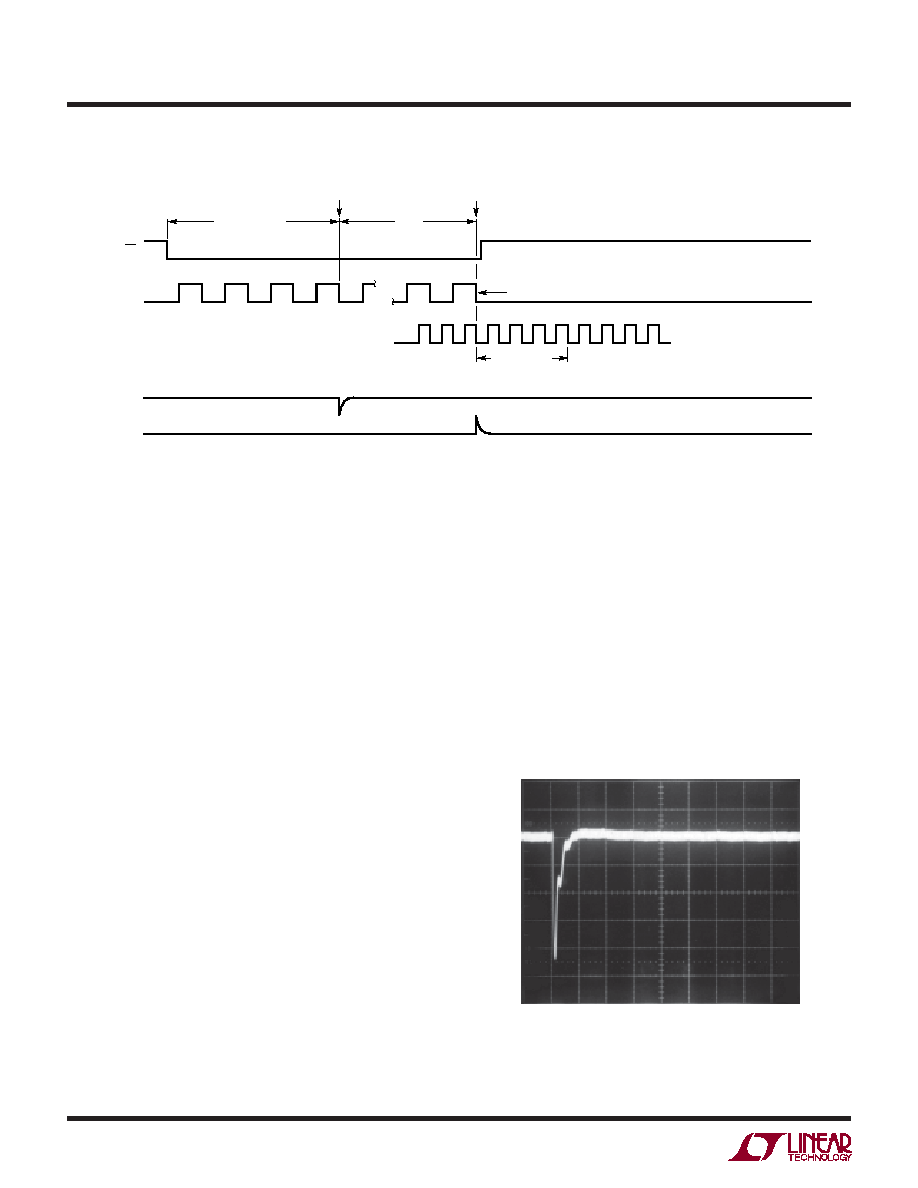
Figure 10. “+” and “–” Input Settling Windows
“+” Input Settling
This input capacitor is switched onto the “+” input during
the sample phase (tSMPL, see Figure 10). The sample
phase starts at the 4th SCLK cycle and lasts until the falling
edge of the last SCLK (the 8th, 10th, 12th or 16th SCLK
cycle depending on the selected word length). The voltage
on the “+” input must settle completely within this sample
time. Minimizing RSOURCE+ and C1 will improve the input
settling time. If large “+” input source resistance must be
used, the sample time can be increased by using a slower
SCLK frequency or selecting a longer word length. With
the minimum possible sample time of 8
μs, RSOURCE+ < 2k
and C1 < 20pF will provide adequate settling.
“–” Input Settling
At the end of the sample phase the input capacitor switches
to the “–” input and the conversion starts (see Figure 10).
During the conversion, the “+” input voltage is effectively
“held” by the sample-and-hold and will not affect the
conversion result. However, it is critical that the “–” input
voltage be free of noise and settle completely during the
first four ACLK cycles of the conversion time. Minimizing
RSOURCE– and C2 will improve settling time. If large “–”
input source resistance must be used, the time allowed for
settling can be extended by using a slower ACLK fre-
quency. At the maximum ACLK rate of 1MHz, RSOURCE–
< 1k and C2 < 20pF will provide adequate settling.
VERTICAL:
5mV/DIV
HORIZONTAL: 1
μs/DIV
Figure 11. Adequate Settling of Op Amp Driving Analog Input
Input Op Amps
When driving the analog inputs with an op amp it is
important that the op amp settle within the allowed time
(see Figure 10). Again, the “+” and “–” input sampling
times can be extended as described above to accommo-
date slower op amps. Most op amps including the LT1006
and LT1013 single supply op amps can be made to settle
well even with the minimum settling windows of 8
μs (“+”
input) and 4
μs (“–” input) which occur at the maximum
clock rates (ACLK = 1MHz and SCLK = 0.5MHz). Figures 11
and 12 show examples of adequate and poor op amp
settling.
SCLK
CS
“+” INPUT
ACLK
LTC1283 F10
1
234
MUX ADDRESS
SHIFTED IN
tSMPL
LAST SCLK (8TH, 10TH, 12TH OR 16TH DEPENDING ON WORD LENGTH)
1
234
1ST BIT TEST
“–” INPUT MUST SETTLE
DURING THIS TIME
SAMPLE
HOLD
“+” INPUT
MUST SETTLE
DURING THIS TIME
“–” INPUT
相关PDF资料 |
PDF描述 |
|---|---|
| D38999/20JJ8PA | CONN RCPT 8POS WALL MNT W/PINS |
| VE-B1J-IU-F3 | CONVERTER MOD DC/DC 36V 200W |
| D38999/20MJ8PN | CONN RCPT 8POS WALL MNT W/PINS |
| LTC1297CCN8#PBF | IC DATA ACQ SYSTEM 12BIT 8-DIP |
| VE-B1J-IU-F2 | CONVERTER MOD DC/DC 36V 200W |
相关代理商/技术参数 |
参数描述 |
|---|---|
| LTC1283ACN#PBF | 功能描述:IC DATA ACQ SYS 10BIT 3V 20-DIP RoHS:是 类别:集成电路 (IC) >> 数据采集 - ADCs/DAC - 专用型 系列:- 产品培训模块:Lead (SnPb) Finish for COTS Obsolescence Mitigation Program 标准包装:50 系列:- 类型:数据采集系统(DAS) 分辨率(位):16 b 采样率(每秒):21.94k 数据接口:MICROWIRE?,QSPI?,串行,SPI? 电压电源:模拟和数字 电源电压:1.8 V ~ 3.6 V 工作温度:-40°C ~ 85°C 安装类型:表面贴装 封装/外壳:40-WFQFN 裸露焊盘 供应商设备封装:40-TQFN-EP(6x6) 包装:托盘 |
| LTC1283CN | 功能描述:IC DATA ACQ SYS 10BIT 3V 20-DIP RoHS:否 类别:集成电路 (IC) >> 数据采集 - ADCs/DAC - 专用型 系列:- 产品培训模块:Lead (SnPb) Finish for COTS Obsolescence Mitigation Program 标准包装:50 系列:- 类型:数据采集系统(DAS) 分辨率(位):16 b 采样率(每秒):21.94k 数据接口:MICROWIRE?,QSPI?,串行,SPI? 电压电源:模拟和数字 电源电压:1.8 V ~ 3.6 V 工作温度:-40°C ~ 85°C 安装类型:表面贴装 封装/外壳:40-WFQFN 裸露焊盘 供应商设备封装:40-TQFN-EP(6x6) 包装:托盘 |
| LTC1283CN#PBF | 功能描述:IC DATA ACQ SYS 10BIT 3V 20-DIP RoHS:是 类别:集成电路 (IC) >> 数据采集 - ADCs/DAC - 专用型 系列:- 产品培训模块:Lead (SnPb) Finish for COTS Obsolescence Mitigation Program 标准包装:50 系列:- 类型:数据采集系统(DAS) 分辨率(位):16 b 采样率(每秒):21.94k 数据接口:MICROWIRE?,QSPI?,串行,SPI? 电压电源:模拟和数字 电源电压:1.8 V ~ 3.6 V 工作温度:-40°C ~ 85°C 安装类型:表面贴装 封装/外壳:40-WFQFN 裸露焊盘 供应商设备封装:40-TQFN-EP(6x6) 包装:托盘 |
| LTC1285CN8 | 功能描述:IC A/D CONV SAMPLING 12BIT 8-DIP RoHS:否 类别:集成电路 (IC) >> 数据采集 - 模数转换器 系列:- 标准包装:1,000 系列:- 位数:16 采样率(每秒):45k 数据接口:串行 转换器数目:2 功率耗散(最大):315mW 电压电源:模拟和数字 工作温度:0°C ~ 70°C 安装类型:表面贴装 封装/外壳:28-SOIC(0.295",7.50mm 宽) 供应商设备封装:28-SOIC W 包装:带卷 (TR) 输入数目和类型:2 个单端,单极 |
| LTC1285CN8#PBF | 功能描述:IC A/D CONV SAMPLING 12BIT 8-DIP RoHS:是 类别:集成电路 (IC) >> 数据采集 - 模数转换器 系列:- 标准包装:1,000 系列:- 位数:16 采样率(每秒):45k 数据接口:串行 转换器数目:2 功率耗散(最大):315mW 电压电源:模拟和数字 工作温度:0°C ~ 70°C 安装类型:表面贴装 封装/外壳:28-SOIC(0.295",7.50mm 宽) 供应商设备封装:28-SOIC W 包装:带卷 (TR) 输入数目和类型:2 个单端,单极 |
发布紧急采购,3分钟左右您将得到回复。