参数资料
| 型号: | LTC1283ACN |
| 厂商: | Linear Technology |
| 文件页数: | 14/24页 |
| 文件大小: | 0K |
| 描述: | IC DATA ACQ SYS 10BIT 3V 20-DIP |
| 标准包装: | 18 |
| 类型: | 数据采集系统(DAS) |
| 分辨率(位): | 10 b |
| 采样率(每秒): | 15k |
| 数据接口: | 串行,并联 |
| 电压电源: | 双 ± |
| 电源电压: | ±3.3V,3 V ~ 3.6 V |
| 工作温度: | 0°C ~ 70°C |
| 安装类型: | 通孔 |
| 封装/外壳: | 20-DIP(0.300",7.62mm) |
| 供应商设备封装: | 20-PDIP |
| 包装: | 管件 |
21
LTC1283
1283fb
U
S
A
O
PPLICATI
WU
U
I FOR ATIO
noise will contribute virtually no uncertainty to the output
code. However, for reduced references, the noise may
become a significant fraction of an LSB and cause unde-
sirable jitter in the output code. For example, with a 1V
reference, this same 200
μV noise is 0.2LSB peak-to-
peak. This will reduce the range of input voltages over
which a stable output code can be achieved by 0.2LSB. If
the reference is further reduced to 200mV, the 200
μV
noise becomes equal to one LSB and a stable code may
be difficult to achieve. In this case averaging readings
may be necessary.
This noise data was taken in a very clean setup. Any setup
induced noise (noise or ripple on VCC, VREF, VIN or V –) will
add to the internal noise. The lower the reference voltage
to be used, the more critical it becomes to have a clean,
noise-free setup.
when operating at low values of VREF because of the
reduced LSB step size and the resulting higher accuracy
requirement placed on the converter. The following factors
must be considered when operating at low VREF values.
1. Conversion speed (ACLK frequency)
2. Offset
3. Noise
Conversion Speed with Reduced VREF
With reduced reference voltages, the LSB step size is
reduced and the LTC1283 internal comparator overdrive
is reduced. With less overdrive, more time is required to
perform a conversion. Therefore, the maximum ACLK
frequency should be reduced when low values of VREF are
used. This is shown in the typical curve of Maximum
Conversion Clock Rate vs Reference Voltage.
Offset with Reduced VREF
The offset of the LTC1283 has a larger effect on the output
code when the A/D is operated with reduced reference
voltage. The offset (which is typically a fixed voltage)
becomes a larger fraction of an LSB as the size of the LSB
is reduced. The typical curve of Unadjusted Offset Error vs
Reference Voltage shows how offset in LSBs is related to
reference voltage for a typical value of VOS. For example,
a VOS of 0.5mV which is 0.2LSB with a 2.5V reference
becomes 0.5LSB with a 1V reference and 2.5LSBs with a
0.2V reference. If this offset is unacceptable, it can be
corrected digitally by the receiving system or by offsetting
the “–” input to the LTC1283.
Noise with Reduced VREF
The total input referred noise of the LTC1283 can be
reduced to approximately 200
μV peak-to-peak using a
ground plane, good bypassing, good layout techniques
and minimizing noise on the reference inputs. This noise
is insignificant with a 2.5V reference but will become a
larger fraction of an LSB as the size of the LSB is reduced.
The typical curve of Noise Error vs Reference Voltage
shows the LSB contribution of this 200
μV of noise.
For operation with a 2.5V reference, the 200
μV noise is
only 0.08LSB peak-to-peak. In this case, the LTC1283
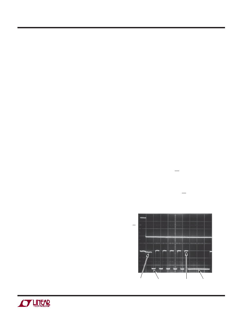
A “Quick Look” Circuit for the LTC1283
Users can get a quick look at the function and timing of the
LTC1283 by using the following simple circuit. REF + and
DIN are tied to VCC selecting a 3V input span, CH7 as a
single-ended input, unipolar mode, MSB-first format and
16-bit word length. ACLK and SCLK are tied together and
driven by an external clock. CS is driven at 1/64 the clock
rate by the CD4520 and DOUT outputs the data. All other
pins are tied to a ground plane. The output data from the
DOUT pin can be viewed on an oscilloscope which is set up
to trigger on the falling edge of CS.
Scope Trace of LTC1283 “Quick Look” Circuit
Showing A/D Output of 0101010101 (155HEX)
VERTICAL: 1V/DIV, HORIZONTAL: 5
μs/DIV
CS
DOUT
MSB
(B9)
DEGLITCHER
TIME
LSB
(B0)
FILLS
ZEROES
相关PDF资料 |
PDF描述 |
|---|---|
| D38999/20JJ8PA | CONN RCPT 8POS WALL MNT W/PINS |
| VE-B1J-IU-F3 | CONVERTER MOD DC/DC 36V 200W |
| D38999/20MJ8PN | CONN RCPT 8POS WALL MNT W/PINS |
| LTC1297CCN8#PBF | IC DATA ACQ SYSTEM 12BIT 8-DIP |
| VE-B1J-IU-F2 | CONVERTER MOD DC/DC 36V 200W |
相关代理商/技术参数 |
参数描述 |
|---|---|
| LTC1283ACN#PBF | 功能描述:IC DATA ACQ SYS 10BIT 3V 20-DIP RoHS:是 类别:集成电路 (IC) >> 数据采集 - ADCs/DAC - 专用型 系列:- 产品培训模块:Lead (SnPb) Finish for COTS Obsolescence Mitigation Program 标准包装:50 系列:- 类型:数据采集系统(DAS) 分辨率(位):16 b 采样率(每秒):21.94k 数据接口:MICROWIRE?,QSPI?,串行,SPI? 电压电源:模拟和数字 电源电压:1.8 V ~ 3.6 V 工作温度:-40°C ~ 85°C 安装类型:表面贴装 封装/外壳:40-WFQFN 裸露焊盘 供应商设备封装:40-TQFN-EP(6x6) 包装:托盘 |
| LTC1283CN | 功能描述:IC DATA ACQ SYS 10BIT 3V 20-DIP RoHS:否 类别:集成电路 (IC) >> 数据采集 - ADCs/DAC - 专用型 系列:- 产品培训模块:Lead (SnPb) Finish for COTS Obsolescence Mitigation Program 标准包装:50 系列:- 类型:数据采集系统(DAS) 分辨率(位):16 b 采样率(每秒):21.94k 数据接口:MICROWIRE?,QSPI?,串行,SPI? 电压电源:模拟和数字 电源电压:1.8 V ~ 3.6 V 工作温度:-40°C ~ 85°C 安装类型:表面贴装 封装/外壳:40-WFQFN 裸露焊盘 供应商设备封装:40-TQFN-EP(6x6) 包装:托盘 |
| LTC1283CN#PBF | 功能描述:IC DATA ACQ SYS 10BIT 3V 20-DIP RoHS:是 类别:集成电路 (IC) >> 数据采集 - ADCs/DAC - 专用型 系列:- 产品培训模块:Lead (SnPb) Finish for COTS Obsolescence Mitigation Program 标准包装:50 系列:- 类型:数据采集系统(DAS) 分辨率(位):16 b 采样率(每秒):21.94k 数据接口:MICROWIRE?,QSPI?,串行,SPI? 电压电源:模拟和数字 电源电压:1.8 V ~ 3.6 V 工作温度:-40°C ~ 85°C 安装类型:表面贴装 封装/外壳:40-WFQFN 裸露焊盘 供应商设备封装:40-TQFN-EP(6x6) 包装:托盘 |
| LTC1285CN8 | 功能描述:IC A/D CONV SAMPLING 12BIT 8-DIP RoHS:否 类别:集成电路 (IC) >> 数据采集 - 模数转换器 系列:- 标准包装:1,000 系列:- 位数:16 采样率(每秒):45k 数据接口:串行 转换器数目:2 功率耗散(最大):315mW 电压电源:模拟和数字 工作温度:0°C ~ 70°C 安装类型:表面贴装 封装/外壳:28-SOIC(0.295",7.50mm 宽) 供应商设备封装:28-SOIC W 包装:带卷 (TR) 输入数目和类型:2 个单端,单极 |
| LTC1285CN8#PBF | 功能描述:IC A/D CONV SAMPLING 12BIT 8-DIP RoHS:是 类别:集成电路 (IC) >> 数据采集 - 模数转换器 系列:- 标准包装:1,000 系列:- 位数:16 采样率(每秒):45k 数据接口:串行 转换器数目:2 功率耗散(最大):315mW 电压电源:模拟和数字 工作温度:0°C ~ 70°C 安装类型:表面贴装 封装/外壳:28-SOIC(0.295",7.50mm 宽) 供应商设备封装:28-SOIC W 包装:带卷 (TR) 输入数目和类型:2 个单端,单极 |
发布紧急采购,3分钟左右您将得到回复。