参数资料
| 型号: | LTC1283ACN |
| 厂商: | Linear Technology |
| 文件页数: | 13/24页 |
| 文件大小: | 0K |
| 描述: | IC DATA ACQ SYS 10BIT 3V 20-DIP |
| 标准包装: | 18 |
| 类型: | 数据采集系统(DAS) |
| 分辨率(位): | 10 b |
| 采样率(每秒): | 15k |
| 数据接口: | 串行,并联 |
| 电压电源: | 双 ± |
| 电源电压: | ±3.3V,3 V ~ 3.6 V |
| 工作温度: | 0°C ~ 70°C |
| 安装类型: | 通孔 |
| 封装/外壳: | 20-DIP(0.300",7.62mm) |
| 供应商设备封装: | 20-PDIP |
| 包装: | 管件 |
20
LTC1283
1283fb
U
S
A
O
PPLICATI
WU
U
I FOR ATIO
differencing operation may not be performed accurately.
The conversion time is 44 ACLK cycles. Therefore, a
change in the “–” input voltage during this interval can
cause conversion errors. For a sinusoidal voltage on the
“–” input this error would be:
VERROR (MAX) = VPEAK × 2 × π × f(“–”) × 44/fACLK
Where f(“–”) is the frequency of the “–” input voltage,
VPEAK is its peak amplitude and fACLK is the frequency of
the ACLK. In most cases VERROR will not be significant. For
a 60Hz signal on the “–” input to generate a 1/4LSB error
(0.61mV) with the converter running at ACLK = 1MHz, its
peak value would have to be 38mV.
5. Reference Inputs
The voltage between the reference inputs of the LTC1283
defines the voltage span of the A/D converter. The refer-
ence inputs look primarily like a 10k resistor but will have
transient capacitive switching currents due to the switched-
capacitor conversion technique (see Figure 14). During
each bit test of the conversion (every 4 ACLK cycles), a
capacitive current spike will be generated on the reference
pins by the A/D. These current spikes settle quickly and do
not cause a problem. However, if slow settling circuitry is
used to drive the reference inputs, care must be taken to
insure that transients caused by these current spikes settle
completely during each bit test of the conversion.
and 16 show examples of both adequate and poor
settling. Using a slower ACLK will allow more time for
the reference to settle. However, even at the maximum
ACLK rate of 1MHz most references and op amps can
be made to settle within the 4
μs bit time.
3. It is recommended that the REF – input be tied directly
to the analog ground plane. If REF – is biased at a
voltage other than ground, the voltage must not change
during a conversion cycle. This voltage must also be
free of noise and ripple with respect to analog ground.
RON
5pF TO 30pF
LTC1283
REF+
ROUT
VREF
EVERY 4 ACLK CYCLES
14
13
REF–
LTC1283 F14
10k
TYP
When driving the reference inputs, three things should be
kept in mind:
1. The source resistance (ROUT) driving the reference
inputs should be low (less than 1
Ω) to prevent DC drops
caused by the 300
μA maximum reference current (IREF).
2. Transients on the reference inputs caused by the
capacitive switching currents must settle completely
during each bit test (each 4 ACLK cycles). Figures 15
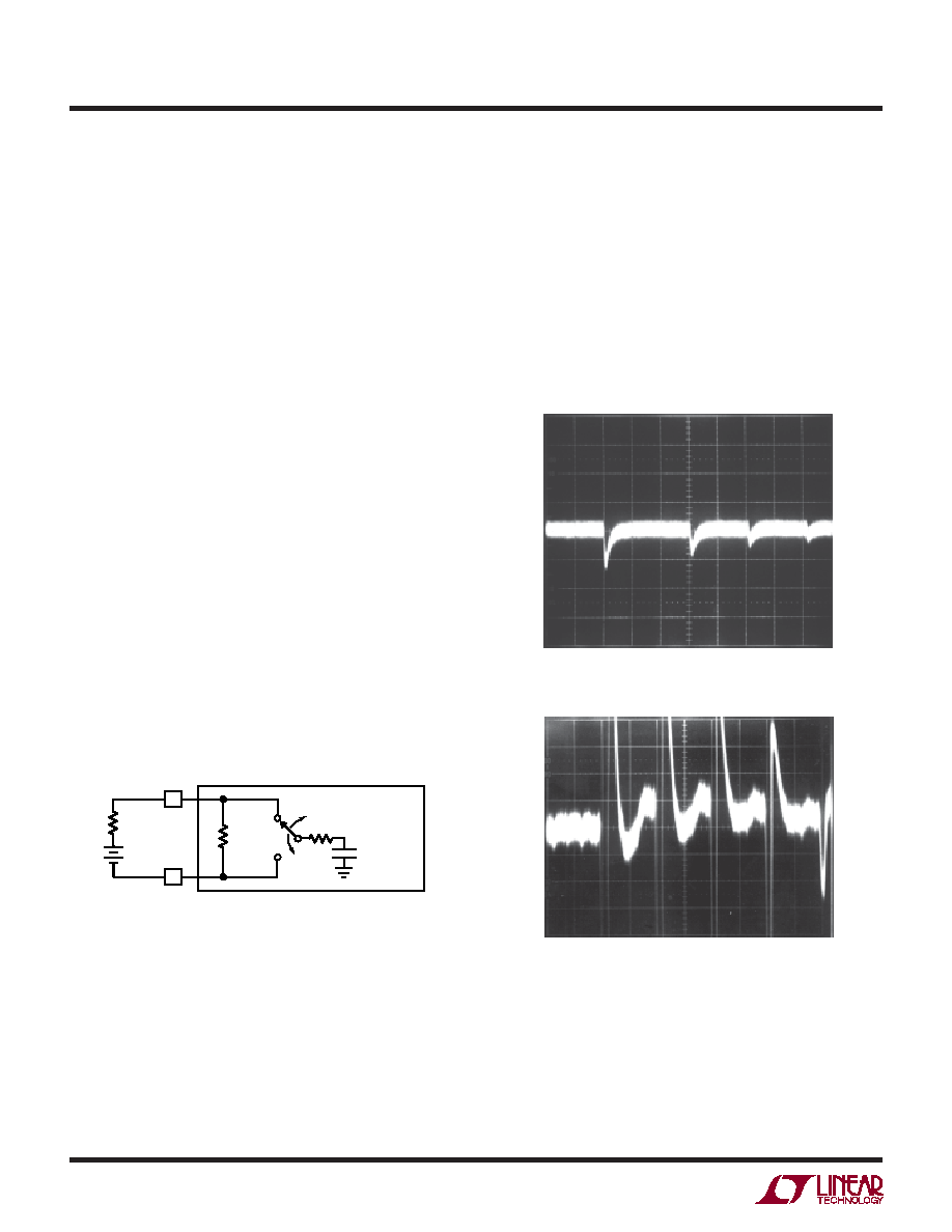
Figure 14. Reference Input Equivalent Circuit
Figure 15. Adequate Reference Settling
6. Reduced Reference Operation
The effective resolution to the LTC1283 can be increased by
reducing the input span of the converter. The LTC1283
exhibits good linearity and gain over a wide range of
reference voltages (see typical curves of Linearity and Gain
Error vs Reference Voltage). However, care must be taken
Figure 16. Poor Reference Settling Can Cause A/D Errors
HORIZONTAL: 1
μs/DIV
VERTICAL:
0.5mV/DIV
VERTICAL:
0.5mV/DIV
HORIZONTAL: 1
μs/DIV
相关PDF资料 |
PDF描述 |
|---|---|
| D38999/20JJ8PA | CONN RCPT 8POS WALL MNT W/PINS |
| VE-B1J-IU-F3 | CONVERTER MOD DC/DC 36V 200W |
| D38999/20MJ8PN | CONN RCPT 8POS WALL MNT W/PINS |
| LTC1297CCN8#PBF | IC DATA ACQ SYSTEM 12BIT 8-DIP |
| VE-B1J-IU-F2 | CONVERTER MOD DC/DC 36V 200W |
相关代理商/技术参数 |
参数描述 |
|---|---|
| LTC1283ACN#PBF | 功能描述:IC DATA ACQ SYS 10BIT 3V 20-DIP RoHS:是 类别:集成电路 (IC) >> 数据采集 - ADCs/DAC - 专用型 系列:- 产品培训模块:Lead (SnPb) Finish for COTS Obsolescence Mitigation Program 标准包装:50 系列:- 类型:数据采集系统(DAS) 分辨率(位):16 b 采样率(每秒):21.94k 数据接口:MICROWIRE?,QSPI?,串行,SPI? 电压电源:模拟和数字 电源电压:1.8 V ~ 3.6 V 工作温度:-40°C ~ 85°C 安装类型:表面贴装 封装/外壳:40-WFQFN 裸露焊盘 供应商设备封装:40-TQFN-EP(6x6) 包装:托盘 |
| LTC1283CN | 功能描述:IC DATA ACQ SYS 10BIT 3V 20-DIP RoHS:否 类别:集成电路 (IC) >> 数据采集 - ADCs/DAC - 专用型 系列:- 产品培训模块:Lead (SnPb) Finish for COTS Obsolescence Mitigation Program 标准包装:50 系列:- 类型:数据采集系统(DAS) 分辨率(位):16 b 采样率(每秒):21.94k 数据接口:MICROWIRE?,QSPI?,串行,SPI? 电压电源:模拟和数字 电源电压:1.8 V ~ 3.6 V 工作温度:-40°C ~ 85°C 安装类型:表面贴装 封装/外壳:40-WFQFN 裸露焊盘 供应商设备封装:40-TQFN-EP(6x6) 包装:托盘 |
| LTC1283CN#PBF | 功能描述:IC DATA ACQ SYS 10BIT 3V 20-DIP RoHS:是 类别:集成电路 (IC) >> 数据采集 - ADCs/DAC - 专用型 系列:- 产品培训模块:Lead (SnPb) Finish for COTS Obsolescence Mitigation Program 标准包装:50 系列:- 类型:数据采集系统(DAS) 分辨率(位):16 b 采样率(每秒):21.94k 数据接口:MICROWIRE?,QSPI?,串行,SPI? 电压电源:模拟和数字 电源电压:1.8 V ~ 3.6 V 工作温度:-40°C ~ 85°C 安装类型:表面贴装 封装/外壳:40-WFQFN 裸露焊盘 供应商设备封装:40-TQFN-EP(6x6) 包装:托盘 |
| LTC1285CN8 | 功能描述:IC A/D CONV SAMPLING 12BIT 8-DIP RoHS:否 类别:集成电路 (IC) >> 数据采集 - 模数转换器 系列:- 标准包装:1,000 系列:- 位数:16 采样率(每秒):45k 数据接口:串行 转换器数目:2 功率耗散(最大):315mW 电压电源:模拟和数字 工作温度:0°C ~ 70°C 安装类型:表面贴装 封装/外壳:28-SOIC(0.295",7.50mm 宽) 供应商设备封装:28-SOIC W 包装:带卷 (TR) 输入数目和类型:2 个单端,单极 |
| LTC1285CN8#PBF | 功能描述:IC A/D CONV SAMPLING 12BIT 8-DIP RoHS:是 类别:集成电路 (IC) >> 数据采集 - 模数转换器 系列:- 标准包装:1,000 系列:- 位数:16 采样率(每秒):45k 数据接口:串行 转换器数目:2 功率耗散(最大):315mW 电压电源:模拟和数字 工作温度:0°C ~ 70°C 安装类型:表面贴装 封装/外壳:28-SOIC(0.295",7.50mm 宽) 供应商设备封装:28-SOIC W 包装:带卷 (TR) 输入数目和类型:2 个单端,单极 |
发布紧急采购,3分钟左右您将得到回复。