- 您现在的位置:买卖IC网 > PDF目录10263 > LTC1285IS8#TRPBF (Linear Technology)IC A/D CONV SAMPLING 12BIT 8SOIC PDF资料下载
参数资料
| 型号: | LTC1285IS8#TRPBF |
| 厂商: | Linear Technology |
| 文件页数: | 4/24页 |
| 文件大小: | 0K |
| 描述: | IC A/D CONV SAMPLING 12BIT 8SOIC |
| 标准包装: | 2,500 |
| 位数: | 12 |
| 采样率(每秒): | 7.5k |
| 数据接口: | MICROWIRE?,串行,SPI? |
| 转换器数目: | 1 |
| 功率耗散(最大): | 480µW |
| 电压电源: | 单电源 |
| 工作温度: | 0°C ~ 70°C |
| 安装类型: | 表面贴装 |
| 封装/外壳: | 8-SOIC(0.154",3.90mm 宽) |
| 供应商设备封装: | 8-SOIC |
| 包装: | 带卷 (TR) |
| 输入数目和类型: | 1 个差分,单极 |
12
LTC1285/LTC1288
Start Bit
The first “logical one” clocked into the DIN input after CS
goes low is the start bit. The start bit initiates the data
transfer. The LTC1288 will ignore all leading zeros which
precede this logical one. After the start bit is received, the
remaining bits of the input word will be clocked in. Further
inputs on the DIN pin are then ignored until the next CS
cycle.
Multiplexer (MUX) Address
The bits of the input word following the START bit assign
the MUX configuration for the requested conversion. For
a given channel selection, the converter will measure the
voltage between the two channels indicated by the “+”
and “–” signs in the selected row of the following tables.
In single-ended mode, all input channels are measured
with respect to GND.
APPLICATION INFORMATION
WU
U
Data Transfer
The CLK synchronizes the data transfer with each bit
being transmitted on the falling CLK edge and captured
on the rising CLK edge in both transmitting and receiving
systems.
The LTC1285 does not require a configuration input word
and has no DIN pin. A falling CS initiates data transfer as
shown in the LTC1285 operating sequence. After CS falls
the second CLK pulse enables DOUT. After one null bit the
A/D conversion result is output on the DOUT line. Bringing
CS high resets the LTC1285 for the next data exchange.
The LTC1288 first receives input data and then transmits
back the A/D conversion result (half duplex). Because of
the half duplex operation, DIN and DOUT may be tied
together allowing transmission over just 3 wires: CS, CLK
and DATA (DIN/DOUT).
Data transfer is initiated by a falling chip select (CS) signal.
After CS falls the LTC1288 looks for a start bit. After the
start bit is received, the 3-bit input word is shifted into the
DIN input which configures the LTC1288 and starts the
conversion. After one null bit, the result of the conversion
is output on the DOUT line. At the end of the data exchange
CS should be brought high. This resets the LTC1288 in
preparation for the next data exchange.
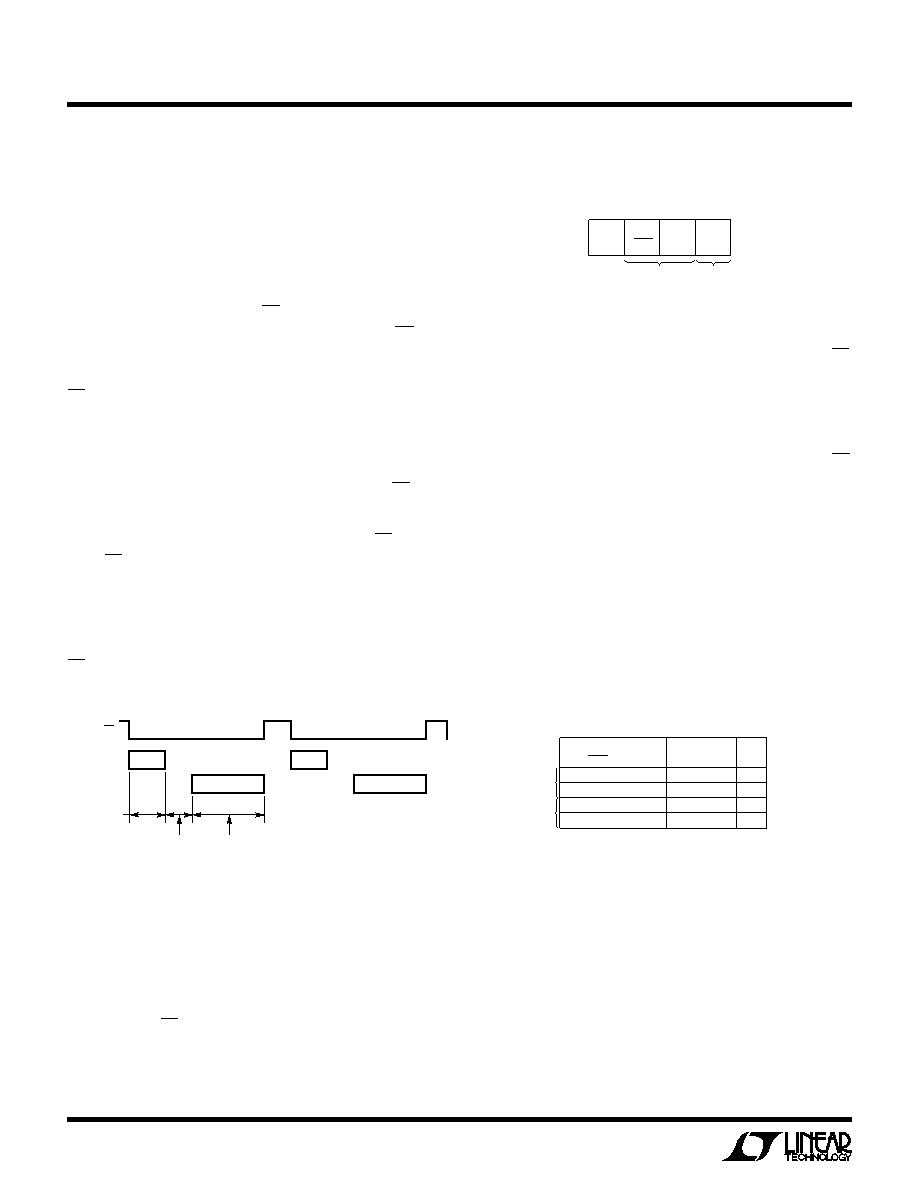
DIN 1
DIN 2
DOUT 1
DOUT 2
CS
SHIFT MUX
ADDRESS IN
1 NULL BIT
SHIFT A/D CONVERSION
RESULT OUT
LTC1285/88 AI01
the rising edge of the clock. The input data words are
defined as follows:
ODD/
SIGN
MSBF
START
MUX
ADDRESS
MSB FIRST/
LSB FIRST
LTC1285/88 AI02
SGL/
DIFF
LTC1288 Channel Selection
MUX ADDRESS
ODD/SIGN
0
1
0
1
CHANNEL #
0
+
–
1
+
–
+
GND
–
SINGLE-ENDED
MUX MODE
DIFFERENTIAL
MUX MODE
LTC1285/88 AI03
SGL/DIFF
1
0
MSB First/LSB First (MSBF)
The output data of the LTC1288 is programmed for
MSB first or LSB first sequence using the MSBF bit.
When the MSBF bit is a logical one, data will appear on
the DOUT line in MSB first format. Logical zeros will be
filled in indefinitely following the last data bit. When the
MSBF bit is a logical zero, LSB first data will follow the
normal MSB first data on the DOUT line (see Operating
Sequence).
Input Data Word
The LTC1285 requires no DIN word. It is permanently
configured to have a single differential input. The conver-
sion result appears on the DOUT line. The data format is
MSB first followed by the LSB sequence. This provides
easy interface to MSB or LSB first serial ports. For MSB
first data the CS signal can be taken high after B0 (see
Figure 1). The LTC1288 clocks data into the DIN input on
相关PDF资料 |
PDF描述 |
|---|---|
| LTC1285IS8#TR | IC ADC 12BIT 3V SAMPLING 8SOIC |
| MAX9761ETI+T | IC AMP AUDIO PWR 3W STER 28TQFN |
| MS27468E11A98P | CONN RCPT 6POS JAM NUT W/PINS |
| MAX9773ETG+T | IC AMP AUDIO PWR 1.8W D 24TQFN |
| MS27466T15B97P | CONN RCPT 12POS WALL MT W/PINS |
相关代理商/技术参数 |
参数描述 |
|---|---|
| LTC1286CN8 | 功能描述:IC A/D CONV SAMPLING 12BIT 8-DIP RoHS:否 类别:集成电路 (IC) >> 数据采集 - 模数转换器 系列:- 标准包装:1,000 系列:- 位数:16 采样率(每秒):45k 数据接口:串行 转换器数目:2 功率耗散(最大):315mW 电压电源:模拟和数字 工作温度:0°C ~ 70°C 安装类型:表面贴装 封装/外壳:28-SOIC(0.295",7.50mm 宽) 供应商设备封装:28-SOIC W 包装:带卷 (TR) 输入数目和类型:2 个单端,单极 |
| LTC1286CN8#PBF | 功能描述:IC A/D CONV SAMPLING 12BIT 8-DIP RoHS:是 类别:集成电路 (IC) >> 数据采集 - 模数转换器 系列:- 标准包装:1 系列:microPOWER™ 位数:8 采样率(每秒):1M 数据接口:串行,SPI? 转换器数目:1 功率耗散(最大):- 电压电源:模拟和数字 工作温度:-40°C ~ 125°C 安装类型:表面贴装 封装/外壳:24-VFQFN 裸露焊盘 供应商设备封装:24-VQFN 裸露焊盘(4x4) 包装:Digi-Reel® 输入数目和类型:8 个单端,单极 产品目录页面:892 (CN2011-ZH PDF) 其它名称:296-25851-6 |
| LTC1286CN8PBF | 制造商:Linear Technology 功能描述:LTC1286CN8PBF |
| LTC1286CS8 | 功能描述:IC A/D CONV SAMPLING 12BIT 8SOIC RoHS:否 类别:集成电路 (IC) >> 数据采集 - 模数转换器 系列:- 标准包装:1,000 系列:- 位数:16 采样率(每秒):45k 数据接口:串行 转换器数目:2 功率耗散(最大):315mW 电压电源:模拟和数字 工作温度:0°C ~ 70°C 安装类型:表面贴装 封装/外壳:28-SOIC(0.295",7.50mm 宽) 供应商设备封装:28-SOIC W 包装:带卷 (TR) 输入数目和类型:2 个单端,单极 |
| LTC1286CS8#PBF | 功能描述:IC A/D CONV SAMPLING 12BIT 8SOIC RoHS:是 类别:集成电路 (IC) >> 数据采集 - 模数转换器 系列:- 标准包装:1 系列:microPOWER™ 位数:8 采样率(每秒):1M 数据接口:串行,SPI? 转换器数目:1 功率耗散(最大):- 电压电源:模拟和数字 工作温度:-40°C ~ 125°C 安装类型:表面贴装 封装/外壳:24-VFQFN 裸露焊盘 供应商设备封装:24-VQFN 裸露焊盘(4x4) 包装:Digi-Reel® 输入数目和类型:8 个单端,单极 产品目录页面:892 (CN2011-ZH PDF) 其它名称:296-25851-6 |
发布紧急采购,3分钟左右您将得到回复。