- 您现在的位置:买卖IC网 > PDF目录10263 > LTC1285IS8#TRPBF (Linear Technology)IC A/D CONV SAMPLING 12BIT 8SOIC PDF资料下载
参数资料
| 型号: | LTC1285IS8#TRPBF |
| 厂商: | Linear Technology |
| 文件页数: | 6/24页 |
| 文件大小: | 0K |
| 描述: | IC A/D CONV SAMPLING 12BIT 8SOIC |
| 标准包装: | 2,500 |
| 位数: | 12 |
| 采样率(每秒): | 7.5k |
| 数据接口: | MICROWIRE?,串行,SPI? |
| 转换器数目: | 1 |
| 功率耗散(最大): | 480µW |
| 电压电源: | 单电源 |
| 工作温度: | 0°C ~ 70°C |
| 安装类型: | 表面贴装 |
| 封装/外壳: | 8-SOIC(0.154",3.90mm 宽) |
| 供应商设备封装: | 8-SOIC |
| 包装: | 带卷 (TR) |
| 输入数目和类型: | 1 个差分,单极 |
14
LTC1285/LTC1288
APPLICATION INFORMATION
WU
U
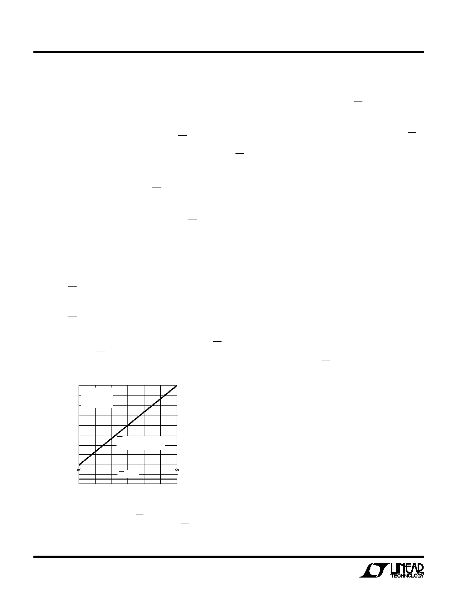
Figure 5. Shutdown Current with CS High is 1nA Typically,
Regardless of the Clock. Shutdown Current with CS = Ground
Varies From 1
A at 1kHz to 9A at 120kHz
Several things must be taken into account to achieve such
a low power consumption.
Shutdown
The LTC1285/LTC1288 are equipped with automatic shut-
down features. They draw power when the CS pin is low
and shut down completely when that pin is high. The bias
circuit and comparator powers down and the reference
input becomes high impedance at the end of each conver-
sion leaving the CLK running to clock out the LSB first data
or zeroes (see Figures 1 and 2). If the CS is not running rail-
to-rail, the input logic buffer will draw current. This current
may be large compared to the typical supply current. To
obtain the lowest supply current, bring the CS pin to
ground when it is low and to supply voltage when it is high.
When the CS pin is high (= supply voltage), the converter
is in shutdown mode and draws only leakage current. The
status of the DIN and CLK input have no effect on supply
current during this time. There is no need to stop DIN and
CLK with CS = high; they can continue to run without
drawing current.
Minimize CS Low Time
In systems that have significant time between conver-
sions, lowest power drain will occur with the minimum CS
low time. Bringing CS low, transferring data as quickly as
possible, and then bringing it back high will result in the
lowest current drain. This minimizes the amount of time
the device draws power. After a conversion the ADC
automatically shuts down even if CS is held low (see
Figures 1 and 2). If the clock is left running to clock out
LSB-data or zero, the logic will draw a small current.
Figure 5 shows that the typical supply current with CS =
ground varies from 1
A at 1kHz to 9A at 120kHz. When
CS = VCC, the logic is gated off and no supply current is
drawn regardless of the clock frequency.
DOUT Loading
Capacitive loading on the digital output can increase
power consumption. A 100pF capacitor on the DOUT pin
can add more than 16.2
A to the supply current at a
120kHz clock frequency. An extra 16.2
A or so of current
goes into charging and discharging the load capacitor. The
same goes for digital lines driven at a high frequency by
any logic. The C
× V × f currents must be evaluated and the
troublesome ones minimized.
OPERATING ON OTHER THAN 3V SUPPLIES
Both the LTC1285 and the LTC1288 operate from a 2.7V
to 6V supply. To operate the LTC1285/LTC1288 on other
than 3V supplies a few things must be kept in mind.
Input Logic Levels
The input logic levels of CS, CLK and DIN are made to
meet TTL on a 3V supply. When the supply voltage varies,
the input logic levels also change. For the LTC1285/
LTC1288 to sample and convert correctly, the digital
inputs have to be in the proper logical low and high levels
relative to the operating supply voltage (see typical curve
of Digital Input Logic Threshold vs Supply Voltage). If
achieving micropower consumption is desirable, the
digital inputs must go rail-to-rail between supply voltage
and ground (see ACHIEVING MICROPOWER PERFOR-
MANCE section).
Clock Frequency
The maximum recommended clock frequency is 120kHz
for the LTC1285/LTC1288 running off a 3V supply. With
the supply voltage changing, the maximum clock fre-
quency for the devices also changes (see the typical curve
FREQUENCY (kHz)
1
0
SUPPLY
CURRENT
(
A)
1
2
3
4
5
6
20
40
60
80
LTC1285/88 TPC03
100
7
8
9
0.002
120
TA = 25°C
VCC = 2.7V
VREF = 2.5V
CS = 0
(AFTER CONVERSION)
CS = VCC
相关PDF资料 |
PDF描述 |
|---|---|
| LTC1285IS8#TR | IC ADC 12BIT 3V SAMPLING 8SOIC |
| MAX9761ETI+T | IC AMP AUDIO PWR 3W STER 28TQFN |
| MS27468E11A98P | CONN RCPT 6POS JAM NUT W/PINS |
| MAX9773ETG+T | IC AMP AUDIO PWR 1.8W D 24TQFN |
| MS27466T15B97P | CONN RCPT 12POS WALL MT W/PINS |
相关代理商/技术参数 |
参数描述 |
|---|---|
| LTC1286CN8 | 功能描述:IC A/D CONV SAMPLING 12BIT 8-DIP RoHS:否 类别:集成电路 (IC) >> 数据采集 - 模数转换器 系列:- 标准包装:1,000 系列:- 位数:16 采样率(每秒):45k 数据接口:串行 转换器数目:2 功率耗散(最大):315mW 电压电源:模拟和数字 工作温度:0°C ~ 70°C 安装类型:表面贴装 封装/外壳:28-SOIC(0.295",7.50mm 宽) 供应商设备封装:28-SOIC W 包装:带卷 (TR) 输入数目和类型:2 个单端,单极 |
| LTC1286CN8#PBF | 功能描述:IC A/D CONV SAMPLING 12BIT 8-DIP RoHS:是 类别:集成电路 (IC) >> 数据采集 - 模数转换器 系列:- 标准包装:1 系列:microPOWER™ 位数:8 采样率(每秒):1M 数据接口:串行,SPI? 转换器数目:1 功率耗散(最大):- 电压电源:模拟和数字 工作温度:-40°C ~ 125°C 安装类型:表面贴装 封装/外壳:24-VFQFN 裸露焊盘 供应商设备封装:24-VQFN 裸露焊盘(4x4) 包装:Digi-Reel® 输入数目和类型:8 个单端,单极 产品目录页面:892 (CN2011-ZH PDF) 其它名称:296-25851-6 |
| LTC1286CN8PBF | 制造商:Linear Technology 功能描述:LTC1286CN8PBF |
| LTC1286CS8 | 功能描述:IC A/D CONV SAMPLING 12BIT 8SOIC RoHS:否 类别:集成电路 (IC) >> 数据采集 - 模数转换器 系列:- 标准包装:1,000 系列:- 位数:16 采样率(每秒):45k 数据接口:串行 转换器数目:2 功率耗散(最大):315mW 电压电源:模拟和数字 工作温度:0°C ~ 70°C 安装类型:表面贴装 封装/外壳:28-SOIC(0.295",7.50mm 宽) 供应商设备封装:28-SOIC W 包装:带卷 (TR) 输入数目和类型:2 个单端,单极 |
| LTC1286CS8#PBF | 功能描述:IC A/D CONV SAMPLING 12BIT 8SOIC RoHS:是 类别:集成电路 (IC) >> 数据采集 - 模数转换器 系列:- 标准包装:1 系列:microPOWER™ 位数:8 采样率(每秒):1M 数据接口:串行,SPI? 转换器数目:1 功率耗散(最大):- 电压电源:模拟和数字 工作温度:-40°C ~ 125°C 安装类型:表面贴装 封装/外壳:24-VFQFN 裸露焊盘 供应商设备封装:24-VQFN 裸露焊盘(4x4) 包装:Digi-Reel® 输入数目和类型:8 个单端,单极 产品目录页面:892 (CN2011-ZH PDF) 其它名称:296-25851-6 |
发布紧急采购,3分钟左右您将得到回复。