- 您现在的位置:买卖IC网 > PDF目录39404 > LTC1289CIJ#TRPBF (LINEAR TECHNOLOGY CORP) 8-CH 12-BIT SUCCESSIVE APPROXIMATION ADC, SERIAL ACCESS, CDIP20 PDF资料下载
参数资料
| 型号: | LTC1289CIJ#TRPBF |
| 厂商: | LINEAR TECHNOLOGY CORP |
| 元件分类: | ADC |
| 英文描述: | 8-CH 12-BIT SUCCESSIVE APPROXIMATION ADC, SERIAL ACCESS, CDIP20 |
| 封装: | 0.300 INCH, LEAD FREE, CERDIP-20 |
| 文件页数: | 13/28页 |
| 文件大小: | 663K |
| 代理商: | LTC1289CIJ#TRPBF |
第1页第2页第3页第4页第5页第6页第7页第8页第9页第10页第11页第12页当前第13页第14页第15页第16页第17页第18页第19页第20页第21页第22页第23页第24页第25页第26页第27页第28页
20
LTC1289
1289fb
U
S
A
O
PPLICATI
WU
U
I FOR ATIO
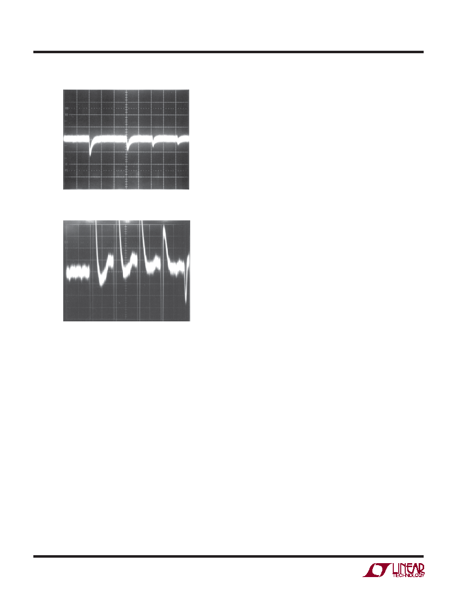
Figure 15. Adequate Reference Settling
HORIZONTAL: 1
s/DIV
VERTICAL:
0.5mV/DIV
2. It is recommended that REF– input be tied directly to
the analog ground plane. If REF– is biased at a voltage
other than ground, the voltage must not change during
a conversion cycle. This voltage must also be free of
noise and ripple with respect to analog ground.
6. Reduced Reference Operation
The effective resolution of the LTC1289 can be increased
by reducing the input span of the converter. The LTC1289
exhibits good linearity and gain over a wide range of
reference voltages (see typical curves of Linearity and Gain
Error vs Reference Voltage). However, care must be taken
when operating at low values of VREF because of the
reduced LSB step size and the resulting higher accuracy
requirement placed on the converter. The following factors
must be considered when operating at low VREF values:
1. Offset
2. Noise
Offset with Reduced VREF
The offset of the LTC1289 has a larger effect on the output
code when the A/D is operated with reduced reference
voltage. The offset (which is typically a fixed voltage)
becomes a larger fraction of an LSB as the size of the LSB
is reduced. The typical curve of Unadjusted Offset Error vs
Reference Voltage shows how offset in LSBs is related to
reference voltage for a typical value of VOS. For example,
a VOS of 0.1mV which is 0.2LSB with a 2.5V reference
becomes 0.4LSB with a 1.25V reference. If this offset is
unacceptable, it can be corrected digitally by the receiving
system or by offsetting the “–” input to the LTC1289.
Noise with Reduced VREF
The total input referred noise of the LTC1289 can be
reduced to approximately 200
V peak-to-peak using a
ground plane, good bypassing, good layout techniques
and minimizing noise on the reference inputs. This noise
is insignificant with a 2.5V reference but will become a
larger fraction of an LSB as the size of the LSB is reduced.
The typical curve of Noise Error vs Reference Voltage
shows the LSB contribution of this 200
V of noise.
For operation with a 2.5 reference, the 200
V noise is only
0.32LSB peak-to-peak. In this case, the LTC1289 noise
will contribute virtually no uncertainty to the output code.
However, for reduced references, the noise may become
a significant fraction of an LSB and cause undesirable jitter
in the output code. For example, with a 1.25V reference,
this same 200
V noise is 0.64LSB peak-to-peak. This will
reduce the range of input voltages over which a stable
output code can be achieved by 0.64LSB. In this case
averaging readings may be necessary.
This noise data was taken in a very clean setup. Any setup
induced noise (noise or ripple on VCC, VREF, VIN or V–) will
add to the internal noise. The lower the reference voltage
to be used, the more critical it becomes to have a clean,
noise-free setup.
Figure 16. Poor Reference Settling Can Cause A/D Errors
HORIZONTAL: 1
s/DIV
VERTICAL:
0.5mV/DIV
相关PDF资料 |
PDF描述 |
|---|---|
| LTC1289BCJ#TRPBF | 8-CH 12-BIT SUCCESSIVE APPROXIMATION ADC, SERIAL ACCESS, CDIP20 |
| LTC1289CIJ#TR | 8-CH 12-BIT SUCCESSIVE APPROXIMATION ADC, SERIAL ACCESS, CDIP20 |
| LTC1289CCN#TR | 8-CH 12-BIT SUCCESSIVE APPROXIMATION ADC, SERIAL ACCESS, PDIP20 |
| LTC1289BCJ#PBF | 8-CH 12-BIT SUCCESSIVE APPROXIMATION ADC, SERIAL ACCESS, CDIP20 |
| LTC1290BCJ | 12-BIT SUCCESSIVE APPROXIMATION ADC, PARALLEL ACCESS, CDIP20 |
相关代理商/技术参数 |
参数描述 |
|---|---|
| LTC1290BCJ | 制造商:Linear Technology 功能描述:ADC Single SAR 50ksps 12-bit Serial 20-Pin CDIP |
| LTC1290BCN | 功能描述:IC DATA ACQ SYS 12BIT 20-DIP RoHS:否 类别:集成电路 (IC) >> 数据采集 - ADCs/DAC - 专用型 系列:- 产品培训模块:Lead (SnPb) Finish for COTS Obsolescence Mitigation Program 标准包装:50 系列:- 类型:数据采集系统(DAS) 分辨率(位):16 b 采样率(每秒):21.94k 数据接口:MICROWIRE?,QSPI?,串行,SPI? 电压电源:模拟和数字 电源电压:1.8 V ~ 3.6 V 工作温度:-40°C ~ 85°C 安装类型:表面贴装 封装/外壳:40-WFQFN 裸露焊盘 供应商设备封装:40-TQFN-EP(6x6) 包装:托盘 |
| LTC1290BCN#PBF | 功能描述:IC DATA ACQ SYS 12BIT 20-DIP RoHS:是 类别:集成电路 (IC) >> 数据采集 - ADCs/DAC - 专用型 系列:- 产品培训模块:Lead (SnPb) Finish for COTS Obsolescence Mitigation Program 标准包装:50 系列:- 类型:数据采集系统(DAS) 分辨率(位):16 b 采样率(每秒):21.94k 数据接口:MICROWIRE?,QSPI?,串行,SPI? 电压电源:模拟和数字 电源电压:1.8 V ~ 3.6 V 工作温度:-40°C ~ 85°C 安装类型:表面贴装 封装/外壳:40-WFQFN 裸露焊盘 供应商设备封装:40-TQFN-EP(6x6) 包装:托盘 |
| LTC1290BCSW | 功能描述:IC DATA ACQ SYS 12BIT 20-SOIC RoHS:否 类别:集成电路 (IC) >> 数据采集 - ADCs/DAC - 专用型 系列:- 产品培训模块:Lead (SnPb) Finish for COTS Obsolescence Mitigation Program 标准包装:50 系列:- 类型:数据采集系统(DAS) 分辨率(位):16 b 采样率(每秒):21.94k 数据接口:MICROWIRE?,QSPI?,串行,SPI? 电压电源:模拟和数字 电源电压:1.8 V ~ 3.6 V 工作温度:-40°C ~ 85°C 安装类型:表面贴装 封装/外壳:40-WFQFN 裸露焊盘 供应商设备封装:40-TQFN-EP(6x6) 包装:托盘 |
| LTC1290BCSW#PBF | 功能描述:IC DATA ACQ SYS 12BIT 20-SOIC RoHS:是 类别:集成电路 (IC) >> 数据采集 - ADCs/DAC - 专用型 系列:- 产品培训模块:Lead (SnPb) Finish for COTS Obsolescence Mitigation Program 标准包装:50 系列:- 类型:数据采集系统(DAS) 分辨率(位):16 b 采样率(每秒):21.94k 数据接口:MICROWIRE?,QSPI?,串行,SPI? 电压电源:模拟和数字 电源电压:1.8 V ~ 3.6 V 工作温度:-40°C ~ 85°C 安装类型:表面贴装 封装/外壳:40-WFQFN 裸露焊盘 供应商设备封装:40-TQFN-EP(6x6) 包装:托盘 |
发布紧急采购,3分钟左右您将得到回复。