- 您现在的位置:买卖IC网 > PDF目录39404 > LTC1289CIJ#TRPBF (LINEAR TECHNOLOGY CORP) 8-CH 12-BIT SUCCESSIVE APPROXIMATION ADC, SERIAL ACCESS, CDIP20 PDF资料下载
参数资料
| 型号: | LTC1289CIJ#TRPBF |
| 厂商: | LINEAR TECHNOLOGY CORP |
| 元件分类: | ADC |
| 英文描述: | 8-CH 12-BIT SUCCESSIVE APPROXIMATION ADC, SERIAL ACCESS, CDIP20 |
| 封装: | 0.300 INCH, LEAD FREE, CERDIP-20 |
| 文件页数: | 28/28页 |
| 文件大小: | 663K |
| 代理商: | LTC1289CIJ#TRPBF |
第1页第2页第3页第4页第5页第6页第7页第8页第9页第10页第11页第12页第13页第14页第15页第16页第17页第18页第19页第20页第21页第22页第23页第24页第25页第26页第27页当前第28页
9
LTC1289
1289fb
U
S
A
O
PPLICATI
WU
U
I FOR ATIO
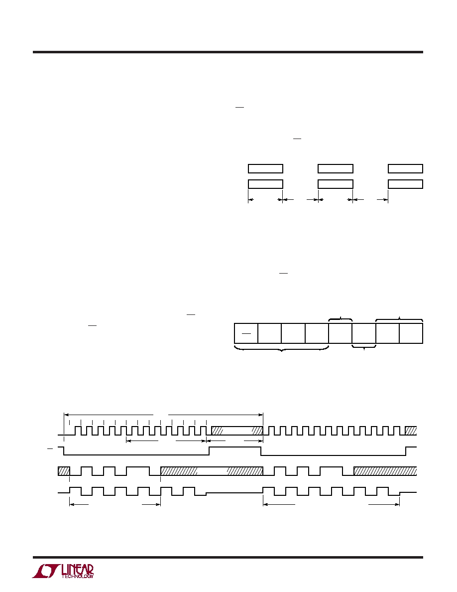
previous conversion is output on the DOUT line. At the end
of the data exchange the requested conversion begins and
CS should be brought high. After tCONV, the conversion is
complete and the results will be available on the next data
transfer cycle. As shown below, the result of a conversion
is delayed by one CS cycle from the input word requesting
it.
Operating Sequence
(Example: Differential Inputs (CH3-CH2), Bipolar, MSB-First and 12-Bit Word Length)
Input Data Word
The LTC1289 8-bit data word is clocked into the DIN input
on the first eight rising SCLK edges after chip select is
recognized. Further inputs on the DIN pin are then ignored
until the next CS cycle. The eight bits of the input word are
defined as follows:
DIN
DOUT DOUT WORD 0
DIN WORD 1
DATA
TRANSFER
DOUT WORD 2
DIN WORD 3
DOUT WORD 1
DIN WORD 2
DATA
TRANSFER
tCONV
A/D
CONVERSION
tCONV
A/D
CONVERSION
LTC1289 AI01
SGL/
DIFF
SELECT
1
SELECT
0
UNI
MSBF
WL1
MUX ADDRESS
MSB-FIRST/
LSB-FIRST
UNIPOLAR/
BIPOLAR
WORD
LENGTH
LTC1289 AI02
ODD/
SIGN
WL0
123456789
10
11
12
tCONV
DON'T CARE
tCYC
SHIFT CONFIGURATION
WORD IN
tSMPL
SHIFT A/D RESULT OUT AND
NEW CONFIGURATION WORD IN
B11 B10 B9
B8
B7
B6
B5
B4
B3
B2
B1
B0
(SB)
LTC1289 AI03
SCLK
DIN
DOUT
CS
The LTC1289 is a data acquisition component which
contains the following functional blocks:
1. 12-bit successive approximation capacitive A/D
converter
2. Analog multiplexer (MUX)
3. Sample-and-hold (S/H)
4. Synchronous, full duplex serial interface
5. Control and timing logic
DIGITAL CONSIDERATIONS
Serial Interface
The LTC1289 communicates with microprocessors and
other external circuitry via a synchronous, full duplex, four
wire serial interface (see Operating Sequence). The shift
clock (SCLK) synchronizes the data transfer with each bit
being transmitted on the falling SCLK edge and captured
on the rising SCLK edge in both transmitting and receiving
systems. The data is transmitted and received simulta-
neously (full duplex).
Data transfer is initiated by a falling chip select (CS) signal.
After the falling CS is recognized, an 8-bit input word is
shifted into the DIN input which configures the LTC1289
for the next conversion. Simultaneously, the result of the
相关PDF资料 |
PDF描述 |
|---|---|
| LTC1289BCJ#TRPBF | 8-CH 12-BIT SUCCESSIVE APPROXIMATION ADC, SERIAL ACCESS, CDIP20 |
| LTC1289CIJ#TR | 8-CH 12-BIT SUCCESSIVE APPROXIMATION ADC, SERIAL ACCESS, CDIP20 |
| LTC1289CCN#TR | 8-CH 12-BIT SUCCESSIVE APPROXIMATION ADC, SERIAL ACCESS, PDIP20 |
| LTC1289BCJ#PBF | 8-CH 12-BIT SUCCESSIVE APPROXIMATION ADC, SERIAL ACCESS, CDIP20 |
| LTC1290BCJ | 12-BIT SUCCESSIVE APPROXIMATION ADC, PARALLEL ACCESS, CDIP20 |
相关代理商/技术参数 |
参数描述 |
|---|---|
| LTC1290BCJ | 制造商:Linear Technology 功能描述:ADC Single SAR 50ksps 12-bit Serial 20-Pin CDIP |
| LTC1290BCN | 功能描述:IC DATA ACQ SYS 12BIT 20-DIP RoHS:否 类别:集成电路 (IC) >> 数据采集 - ADCs/DAC - 专用型 系列:- 产品培训模块:Lead (SnPb) Finish for COTS Obsolescence Mitigation Program 标准包装:50 系列:- 类型:数据采集系统(DAS) 分辨率(位):16 b 采样率(每秒):21.94k 数据接口:MICROWIRE?,QSPI?,串行,SPI? 电压电源:模拟和数字 电源电压:1.8 V ~ 3.6 V 工作温度:-40°C ~ 85°C 安装类型:表面贴装 封装/外壳:40-WFQFN 裸露焊盘 供应商设备封装:40-TQFN-EP(6x6) 包装:托盘 |
| LTC1290BCN#PBF | 功能描述:IC DATA ACQ SYS 12BIT 20-DIP RoHS:是 类别:集成电路 (IC) >> 数据采集 - ADCs/DAC - 专用型 系列:- 产品培训模块:Lead (SnPb) Finish for COTS Obsolescence Mitigation Program 标准包装:50 系列:- 类型:数据采集系统(DAS) 分辨率(位):16 b 采样率(每秒):21.94k 数据接口:MICROWIRE?,QSPI?,串行,SPI? 电压电源:模拟和数字 电源电压:1.8 V ~ 3.6 V 工作温度:-40°C ~ 85°C 安装类型:表面贴装 封装/外壳:40-WFQFN 裸露焊盘 供应商设备封装:40-TQFN-EP(6x6) 包装:托盘 |
| LTC1290BCSW | 功能描述:IC DATA ACQ SYS 12BIT 20-SOIC RoHS:否 类别:集成电路 (IC) >> 数据采集 - ADCs/DAC - 专用型 系列:- 产品培训模块:Lead (SnPb) Finish for COTS Obsolescence Mitigation Program 标准包装:50 系列:- 类型:数据采集系统(DAS) 分辨率(位):16 b 采样率(每秒):21.94k 数据接口:MICROWIRE?,QSPI?,串行,SPI? 电压电源:模拟和数字 电源电压:1.8 V ~ 3.6 V 工作温度:-40°C ~ 85°C 安装类型:表面贴装 封装/外壳:40-WFQFN 裸露焊盘 供应商设备封装:40-TQFN-EP(6x6) 包装:托盘 |
| LTC1290BCSW#PBF | 功能描述:IC DATA ACQ SYS 12BIT 20-SOIC RoHS:是 类别:集成电路 (IC) >> 数据采集 - ADCs/DAC - 专用型 系列:- 产品培训模块:Lead (SnPb) Finish for COTS Obsolescence Mitigation Program 标准包装:50 系列:- 类型:数据采集系统(DAS) 分辨率(位):16 b 采样率(每秒):21.94k 数据接口:MICROWIRE?,QSPI?,串行,SPI? 电压电源:模拟和数字 电源电压:1.8 V ~ 3.6 V 工作温度:-40°C ~ 85°C 安装类型:表面贴装 封装/外壳:40-WFQFN 裸露焊盘 供应商设备封装:40-TQFN-EP(6x6) 包装:托盘 |
发布紧急采购,3分钟左右您将得到回复。