- 您现在的位置:买卖IC网 > PDF目录39404 > LTC1289CIJ#TRPBF (LINEAR TECHNOLOGY CORP) 8-CH 12-BIT SUCCESSIVE APPROXIMATION ADC, SERIAL ACCESS, CDIP20 PDF资料下载
参数资料
| 型号: | LTC1289CIJ#TRPBF |
| 厂商: | LINEAR TECHNOLOGY CORP |
| 元件分类: | ADC |
| 英文描述: | 8-CH 12-BIT SUCCESSIVE APPROXIMATION ADC, SERIAL ACCESS, CDIP20 |
| 封装: | 0.300 INCH, LEAD FREE, CERDIP-20 |
| 文件页数: | 9/28页 |
| 文件大小: | 663K |
| 代理商: | LTC1289CIJ#TRPBF |
第1页第2页第3页第4页第5页第6页第7页第8页当前第9页第10页第11页第12页第13页第14页第15页第16页第17页第18页第19页第20页第21页第22页第23页第24页第25页第26页第27页第28页
17
LTC1289
1289fb
U
S
A
O
PPLICATI
WU
U
I FOR ATIO
3. Analog Inputs
Because of the capacitive redistribution A/D conversion
techniques used, the analog inputs of the LTC1289 have
capacitive switching input current spikes. These current
spikes settle quickly and do not cause a problem. How-
ever, if large source resistances are used or if slow settling
op amps drive the inputs, care must be taken to insure that
the transients caused by the current spikes settle com-
pletely before the conversion begins.
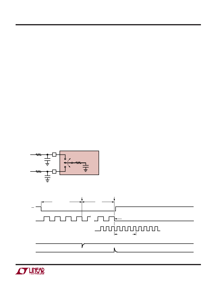
Source Resistance
The analog inputs of the LTC1289 look like a 100pF
capacitor (CIN) is series with a 1500 resistor (RON) as
shown in Figure 9. This value for RON is for VCC = 2.7V.
With larger supply voltages RON will be reduced. For
example with VCC = 2.7V and V –= –2.7V RON becomes
500
. CIN gets switched between the selected “+” and “–”
inputs once during each conversion cycle. Large external
source resistors and capacitances will slow the settling of
Figure 10. “+” and “–” Input Settling Windows
the inputs. It is important that the overall RC time con-
stants be short enough to allow the analog inputs to
completely settle within the allotted time.
“+” Input Settling
This input capacitor is switched onto the “+” input during
the sample phase (tSMPL, see Figure 10). The sample
phase starts at the 4th SCLK cycle and lasts until the falling
edge of the last SCLK (the 8th, 12th or 16th SCLK cycle
depending on the selected word length). The voltage on
the “+” input must settle completely within this sample
time. Minimizing RSOURCE+ and C1 will improve the input
settling time. If large “+” input source resistance must be
used, the sample time can be increased by using a slower
SCLK frequency or selecting a longer word length. With
the minimum possible sample time of 4
s, RSOURCE+ < 2k
and C1 < 20pF will provide adequate settling.
“–” Input Settling
At the end of the sample phase the input capacitor switches
to the “–” input and the conversion starts (see Figure 10).
During the conversion, the “+” input voltage is effectively
“held” by the sample and hold and will not affect the
conversion result. However, it is critical that the “–” input
voltage be free of noise and settle completely during the
first four ACLK cycles of the conversion time. Minimizing
RSOURCE– and C2 will improve settling time. If large “–”
input source resistance must be used, the time allowed for
Figure 9. Analog Input Equivalent Circuit
SCLK
CS
“+” INPUT
ACLK
1289 AIF10
1
234
MUX ADDRESS
SHIFTED IN
tSMPL
LAST SCLK (8TH, 12TH OR 16TH DEPENDING ON WORK LENGTH)
1
234
1ST BIT TEST
“–” INPUT MUST SETTLE
DURING THIS TIME
SAMPLE
HOLD
“+” INPUT
MUST SETTLE
DURING THIS TIME
“–” INPUT
4TH SCLK
RON = 1.5k
LAST SCLK
CIN =
100pF
LTC1289
“+”
INPUT
RSOURCE +
VIN +
C1
“–”
INPUT
RSOURCE –
VIN –
C2
LTC1289 AIF09
相关PDF资料 |
PDF描述 |
|---|---|
| LTC1289BCJ#TRPBF | 8-CH 12-BIT SUCCESSIVE APPROXIMATION ADC, SERIAL ACCESS, CDIP20 |
| LTC1289CIJ#TR | 8-CH 12-BIT SUCCESSIVE APPROXIMATION ADC, SERIAL ACCESS, CDIP20 |
| LTC1289CCN#TR | 8-CH 12-BIT SUCCESSIVE APPROXIMATION ADC, SERIAL ACCESS, PDIP20 |
| LTC1289BCJ#PBF | 8-CH 12-BIT SUCCESSIVE APPROXIMATION ADC, SERIAL ACCESS, CDIP20 |
| LTC1290BCJ | 12-BIT SUCCESSIVE APPROXIMATION ADC, PARALLEL ACCESS, CDIP20 |
相关代理商/技术参数 |
参数描述 |
|---|---|
| LTC1290BCJ | 制造商:Linear Technology 功能描述:ADC Single SAR 50ksps 12-bit Serial 20-Pin CDIP |
| LTC1290BCN | 功能描述:IC DATA ACQ SYS 12BIT 20-DIP RoHS:否 类别:集成电路 (IC) >> 数据采集 - ADCs/DAC - 专用型 系列:- 产品培训模块:Lead (SnPb) Finish for COTS Obsolescence Mitigation Program 标准包装:50 系列:- 类型:数据采集系统(DAS) 分辨率(位):16 b 采样率(每秒):21.94k 数据接口:MICROWIRE?,QSPI?,串行,SPI? 电压电源:模拟和数字 电源电压:1.8 V ~ 3.6 V 工作温度:-40°C ~ 85°C 安装类型:表面贴装 封装/外壳:40-WFQFN 裸露焊盘 供应商设备封装:40-TQFN-EP(6x6) 包装:托盘 |
| LTC1290BCN#PBF | 功能描述:IC DATA ACQ SYS 12BIT 20-DIP RoHS:是 类别:集成电路 (IC) >> 数据采集 - ADCs/DAC - 专用型 系列:- 产品培训模块:Lead (SnPb) Finish for COTS Obsolescence Mitigation Program 标准包装:50 系列:- 类型:数据采集系统(DAS) 分辨率(位):16 b 采样率(每秒):21.94k 数据接口:MICROWIRE?,QSPI?,串行,SPI? 电压电源:模拟和数字 电源电压:1.8 V ~ 3.6 V 工作温度:-40°C ~ 85°C 安装类型:表面贴装 封装/外壳:40-WFQFN 裸露焊盘 供应商设备封装:40-TQFN-EP(6x6) 包装:托盘 |
| LTC1290BCSW | 功能描述:IC DATA ACQ SYS 12BIT 20-SOIC RoHS:否 类别:集成电路 (IC) >> 数据采集 - ADCs/DAC - 专用型 系列:- 产品培训模块:Lead (SnPb) Finish for COTS Obsolescence Mitigation Program 标准包装:50 系列:- 类型:数据采集系统(DAS) 分辨率(位):16 b 采样率(每秒):21.94k 数据接口:MICROWIRE?,QSPI?,串行,SPI? 电压电源:模拟和数字 电源电压:1.8 V ~ 3.6 V 工作温度:-40°C ~ 85°C 安装类型:表面贴装 封装/外壳:40-WFQFN 裸露焊盘 供应商设备封装:40-TQFN-EP(6x6) 包装:托盘 |
| LTC1290BCSW#PBF | 功能描述:IC DATA ACQ SYS 12BIT 20-SOIC RoHS:是 类别:集成电路 (IC) >> 数据采集 - ADCs/DAC - 专用型 系列:- 产品培训模块:Lead (SnPb) Finish for COTS Obsolescence Mitigation Program 标准包装:50 系列:- 类型:数据采集系统(DAS) 分辨率(位):16 b 采样率(每秒):21.94k 数据接口:MICROWIRE?,QSPI?,串行,SPI? 电压电源:模拟和数字 电源电压:1.8 V ~ 3.6 V 工作温度:-40°C ~ 85°C 安装类型:表面贴装 封装/外壳:40-WFQFN 裸露焊盘 供应商设备封装:40-TQFN-EP(6x6) 包装:托盘 |
发布紧急采购,3分钟左右您将得到回复。