- 您现在的位置:买卖IC网 > PDF目录2003 > LTC1298IS8#TRPBF (Linear Technology)IC A/D CONV SAMPLING 12BIT 8SOIC PDF资料下载
参数资料
| 型号: | LTC1298IS8#TRPBF |
| 厂商: | Linear Technology |
| 文件页数: | 10/24页 |
| 文件大小: | 0K |
| 描述: | IC A/D CONV SAMPLING 12BIT 8SOIC |
| 标准包装: | 2,500 |
| 位数: | 12 |
| 采样率(每秒): | 11.1k |
| 数据接口: | MICROWIRE?,串行,SPI? |
| 转换器数目: | 1 |
| 功率耗散(最大): | 1.8mW |
| 电压电源: | 单电源 |
| 工作温度: | -40°C ~ 85°C |
| 安装类型: | 表面贴装 |
| 封装/外壳: | 8-SOIC(0.154",3.90mm 宽) |
| 供应商设备封装: | 8-SOIC |
| 包装: | 带卷 (TR) |
| 输入数目和类型: | 2 个单端,单极 |
18
LTC1286/LTC1298
0.2V reference. If this offset is unacceptable, it can be
corrected digitally by the receiving system or by offsetting
the “–” input of the LTC1286.
Noise with Reduced VREF
The total input referred noise of the LTC1286 can be
reduced to approximately 400
V peak-to-peak using a
ground plane, good bypassing, good layout techniques
and minimizing noise on the reference inputs. This noise
is insignificant with a 5V reference but will become a larger
fraction of an LSB as the size of the LSB is reduced.
For operation with a 5V reference, the 400
V noise is
only 0.33LSB peak-to-peak. In this case, the LTC1286
noise will contribute virtually no uncertainty to the
output code. However, for reduced references the noise
may become a significant fraction of an LSB and cause
undesirable jitter in the output code. For example, with
a 2.5V reference this same 400
V noise is 0.66LSB
peak-to-peak. This will reduce the range of input volt-
ages over which a stable output code can be achieved by
1LSB. If the reference is further reduced to 1V, the 400
V
noise becomes equal to 1.65LSBs and a stable code may
be difficult to achieve. In this case averaging multiple
readings may be necessary.
This noise data was taken in a very clean setup. Any setup
induced noise (noise or ripple on VCC, VREF or VIN) will add
to the internal noise. The lower the reference voltage to be
used the more critical it becomes to have a clean, noise free
setup.
Conversion Speed with Reduced VREF
With reduced reference voltages, the LSB step size is
reduced and the LTC1286 internal comparator over-
drive is reduced. Therefore, it may be necessary to
reduce the maximum CLK frequency when low values
of VREF are used.
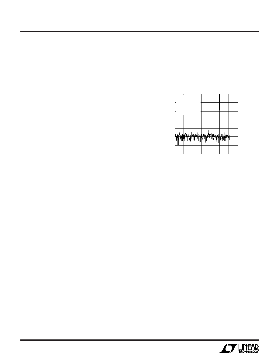
DYNAMIC PERFORMANCE
The LTC1286/LTC1298 have exceptional sampling capa-
bility. Fast Fourier Transform (FFT) test techniques are
used to characterize the ADC’s frequency response, dis-
APPLICATION INFORMATION
WU
U
tortion and noise at the rated throughput. By applying a low
distortion sine wave and analyzing the digital output using
an FFT algorithm, the ADC’s spectral content can be
examined for frequencies outside the fundamental. Figure
11 shows a typical LTC1286 plot.
Signal-to-Noise Ratio
The Signal-to-Noise plus Distortion Ratio (S/N + D) is the
ratio between the RMS amplitude of the fundamental
input frequency to the RMS amplitude of all other fre-
quency components at the ADC’s output. The output is
band limited to frequencies above DC and below one half
the sampling frequency. Figure 12 shows a typical spec-
tral content with a 12.5kHz sampling rate.
Effective Number of Bits
The Effective Number of Bits (ENOBs) is a measurement of
the resolution of an ADC and is directly related to S/(N+D)
by the equation:
ENOB = [S/(N + D) – 1.76]/6.02
where S/(N + D) is expressed in dB. At the maximum
sampling rate of 12.5kHz with a 5V supply, the LTC1286
maintains above 11 ENOBs at 10kHz input frequency.
Above 10kHz the ENOBs gradually decline, as shown in
Figure 12, due to increasing second harmonic distortion.
The noise floor remains low.
FREQUENCY (kHz)
0
–60
–40
0
35
LTC 1286/98 G21
–80
–100
12
46
7
–120
–140
–20
MAGNITUDE
(dB)
TA = 25°C
VCC = VREF = 5V
fIN = 5kHz
fCLK = 200kHz
fSMPL = 12.5kHz
Figure 11. LTC1286 Non-Averaged, 4096 Point FFT Plot
相关PDF资料 |
PDF描述 |
|---|---|
| LTC1327CNW#PBF | IC TXRX EIA/TIA-562 3.3V 28-DIP |
| LTC1329ACS8-50#TRPBF | IC D/A CONV 8BIT MICROPWR 8-SOIC |
| LTC1337CNW#PBF | IC 3DVR/5RCVR 5V RS232 28-DIP |
| LTC1382IN#PBF | IC TXRX 5V RS232 W/SHTDWN 18-DIP |
| LTC1383IS#TRPBF | IC TXRX 5V RS232 LOW PWR 16-SOIC |
相关代理商/技术参数 |
参数描述 |
|---|---|
| LTC1314CS | 功能描述:IC PCMCIA SWITCHNG MATRIX 14SOIC RoHS:否 类别:集成电路 (IC) >> PMIC - 电源分配开关 系列:- 特色产品:XRP252 Switches 标准包装:1 系列:- 类型:高端开关 输出数:2 Rds(开):140 毫欧 内部开关:是 电流限制:1.15A 输入电压:1.75 V ~ 5.5 V 工作温度:-40°C ~ 85°C 安装类型:表面贴装 封装/外壳:10-WFDFN 裸露焊盘 供应商设备封装:10-TDFN(3x3) 包装:Digi-Reel® 其它名称:1016-1691-6 |
| LTC1314CS#PBF | 功能描述:IC PCMCIA SWITCHNG MATRIX 14SOIC RoHS:是 类别:集成电路 (IC) >> PMIC - 电源分配开关 系列:- 特色产品:XRP252 Switches 标准包装:1 系列:- 类型:高端开关 输出数:2 Rds(开):140 毫欧 内部开关:是 电流限制:1.15A 输入电压:1.75 V ~ 5.5 V 工作温度:-40°C ~ 85°C 安装类型:表面贴装 封装/外壳:10-WFDFN 裸露焊盘 供应商设备封装:10-TDFN(3x3) 包装:Digi-Reel® 其它名称:1016-1691-6 |
| LTC1314CS#TR | 功能描述:IC SW MATRIX PCMCIA SGL 14SOIC RoHS:否 类别:集成电路 (IC) >> PMIC - 电源分配开关 系列:- 特色产品:XRP252 Switches 标准包装:1 系列:- 类型:高端开关 输出数:2 Rds(开):140 毫欧 内部开关:是 电流限制:1.15A 输入电压:1.75 V ~ 5.5 V 工作温度:-40°C ~ 85°C 安装类型:表面贴装 封装/外壳:10-WFDFN 裸露焊盘 供应商设备封装:10-TDFN(3x3) 包装:Digi-Reel® 其它名称:1016-1691-6 |
| LTC1314CS#TRPBF | 功能描述:IC PCMCIA SWITCHNG MATRIX 14SOIC RoHS:是 类别:集成电路 (IC) >> PMIC - 电源分配开关 系列:- 特色产品:XRP252 Switches 标准包装:1 系列:- 类型:高端开关 输出数:2 Rds(开):140 毫欧 内部开关:是 电流限制:1.15A 输入电压:1.75 V ~ 5.5 V 工作温度:-40°C ~ 85°C 安装类型:表面贴装 封装/外壳:10-WFDFN 裸露焊盘 供应商设备封装:10-TDFN(3x3) 包装:Digi-Reel® 其它名称:1016-1691-6 |
| LTC1315CG#PBF | 功能描述:IC PCMCIA SWITCHNG MATRIX 24SSOP RoHS:是 类别:集成电路 (IC) >> PMIC - 电源分配开关 系列:- 标准包装:80 系列:- 类型:USB 开关 输出数:2 Rds(开):135 毫欧 内部开关:是 电流限制:1.5A 输入电压:2.7 V ~ 5.5 V 工作温度:-40°C ~ 85°C 安装类型:表面贴装 封装/外壳:8-TSSOP,8-MSOP(0.118",3.00mm 宽)裸露焊盘 供应商设备封装:8-MSOP-PowerPad 包装:管件 配用:TPS2066-1EVM-296-ND - TPS2066-1EVM-296 |
发布紧急采购,3分钟左右您将得到回复。