- 您现在的位置:买卖IC网 > PDF目录2003 > LTC1298IS8#TRPBF (Linear Technology)IC A/D CONV SAMPLING 12BIT 8SOIC PDF资料下载
参数资料
| 型号: | LTC1298IS8#TRPBF |
| 厂商: | Linear Technology |
| 文件页数: | 8/24页 |
| 文件大小: | 0K |
| 描述: | IC A/D CONV SAMPLING 12BIT 8SOIC |
| 标准包装: | 2,500 |
| 位数: | 12 |
| 采样率(每秒): | 11.1k |
| 数据接口: | MICROWIRE?,串行,SPI? |
| 转换器数目: | 1 |
| 功率耗散(最大): | 1.8mW |
| 电压电源: | 单电源 |
| 工作温度: | -40°C ~ 85°C |
| 安装类型: | 表面贴装 |
| 封装/外壳: | 8-SOIC(0.154",3.90mm 宽) |
| 供应商设备封装: | 8-SOIC |
| 包装: | 带卷 (TR) |
| 输入数目和类型: | 2 个单端,单极 |
16
LTC1286/LTC1298
APPLICATION INFORMATION
WU
U
Differential Inputs
With differential inputs, the ADC no longer converts just a
single voltage but rather the difference between two volt-
ages. In this case, the voltage on the selected “+” input is
still sampled and held and therefore may be rapidly time
varying just as in single-ended mode. However, the volt-
age on the selected “–” input must remain constant and be
free of noise and ripple throughout the conversion time.
Otherwise, the differencing operation may not be per-
formed accurately. The conversion time is 12 CLK cycles.
Therefore, a change in the “–” input voltage during this
interval can cause conversion errors. For a sinusoidal
voltage on the “–” input this error would be:
VERROR (MAX) = VPEAK × 2 × π × f(“–”) × 12/fCLK
Where f(“–”) is the frequency of the “–” input voltage,
VPEAK is its peak amplitude and fCLK is the frequency of the
CLK. In most cases VERROR will not be significant. For a
60Hz signal on the “–” input to generate a 1/4LSB error
(305
V) with the converter running at CLK = 200kHz, its
peak value would have to be 13.48mV.
ANALOG INPUTS
Because of the capacitive redistribution A/D conversion
techniques used, the analog inputs of the LTC1286/
LTC1298 have capacitive switching input current spikes.
These current spikes settle quickly and do not cause a
problem. However, if large source resistances are used or
if slow settling op amps drive the inputs, care must be
taken to insure that the transients caused by the current
spikes settle completely before the conversion begins.
“+” Input Settling
The input capacitor of the LTC1286 is switched onto “+”
input during the tSMPL time (see Figure 1) and samples the
input signal within that time. However, the input capacitor
of the LTC1298 is switched onto “+” input during the
sample phase (tSMPL, see Figure 7). The sample phase is
1 1/2 CLK cycles before conversion starts. The voltage on
the “+” input must settle completely within tSMPLE for the
LTC1286 and the LTC1298 respectively. Minimizing
RSOURCE+ and C1 will improve the input settling time. If a
large “+” input source resistance must be used, the
sample time can be increased by using a slower CLK
frequency.
“–” Input Settling
At the end of the tSMPL, the input capacitor switches to the
“–” input and conversion starts (see Figures 1 and 7).
During the conversion, the “+” input voltage is effectively
“held” by the sample-and-hold and will not affect the
conversion result. However, it is critical that the “–” input
voltage settles completely during the first CLK cycle of the
conversion time and be free of noise. Minimizing RSOURCE–
and C2 will improve settling time. If a large “–” input
source resistance must be used, the time allowed for
settling can be extended by using a slower CLK frequency.
Input Op Amps
When driving the analog inputs with an op amp it is
important that the op amp settle within the allowed time
(see Figure 7). Again, the“+” and “–” input sampling times
can be extended as described above to accommodate
slower op amps. Most op amps, including the LT1006 and
LT1413 single supply op amps, can be made to settle well
even with the minimum settling windows of 6
s (“+”
input) which occur at the maximum clock rate of 200kHz.
Source Resistance
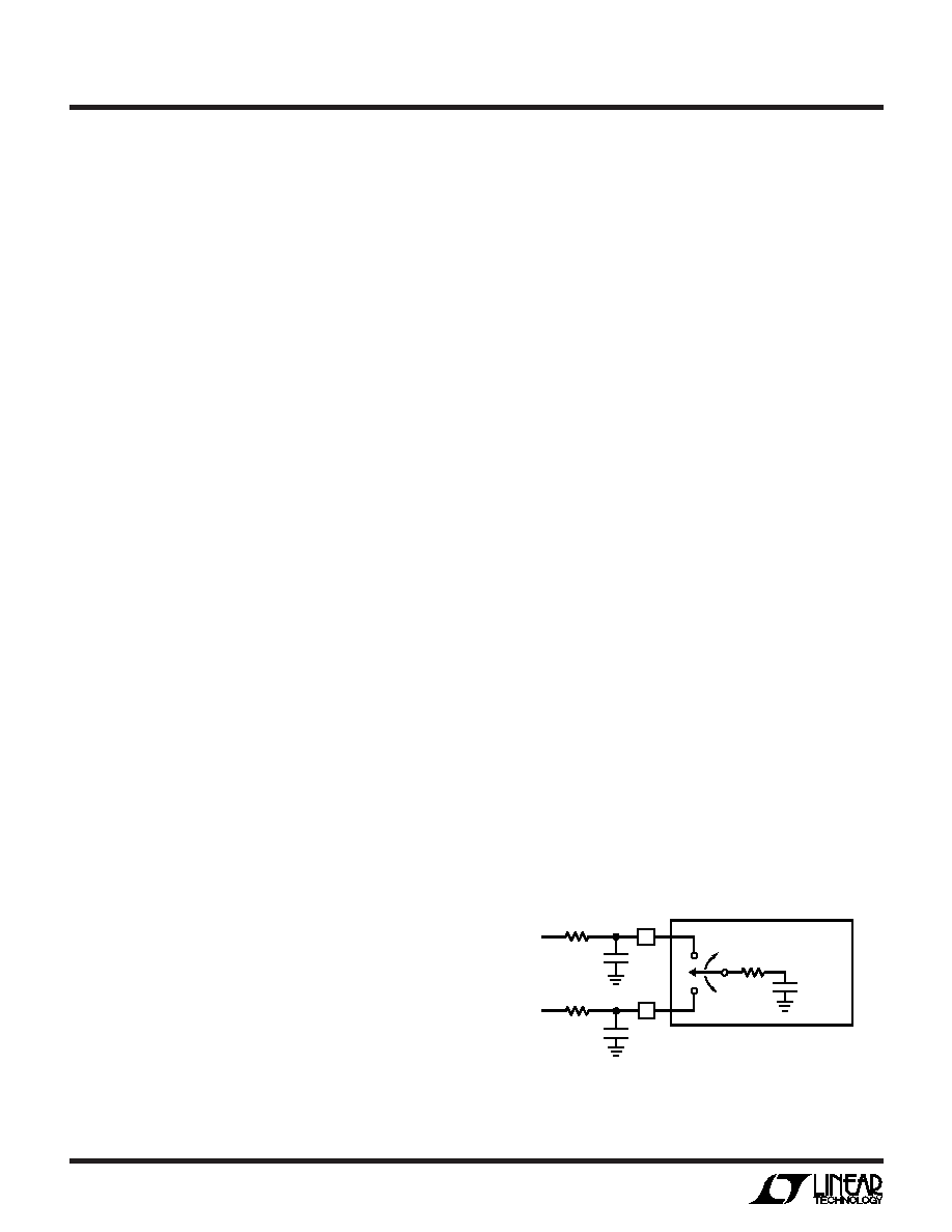
The analog inputs of the LTC1286/LTC1298 look like a
20pF capacitor (CIN) in series with a 500 resistor (RON)
as shown in Figure 8. CIN gets switched between the
selected “+” and “–” inputs once during each conversion
cycle. Large external source resistors and capacitances
Figure 8. Analog Input Equivalent Circuit
RON = 500
CIN = 20pF
LTC1286/98
“+”
INPUT
RSOURCE
+
VIN +
C1
“–”
INPUT
RSOURCE
–
VIN –
C2
LTC1286/98 F08
相关PDF资料 |
PDF描述 |
|---|---|
| LTC1327CNW#PBF | IC TXRX EIA/TIA-562 3.3V 28-DIP |
| LTC1329ACS8-50#TRPBF | IC D/A CONV 8BIT MICROPWR 8-SOIC |
| LTC1337CNW#PBF | IC 3DVR/5RCVR 5V RS232 28-DIP |
| LTC1382IN#PBF | IC TXRX 5V RS232 W/SHTDWN 18-DIP |
| LTC1383IS#TRPBF | IC TXRX 5V RS232 LOW PWR 16-SOIC |
相关代理商/技术参数 |
参数描述 |
|---|---|
| LTC1314CS | 功能描述:IC PCMCIA SWITCHNG MATRIX 14SOIC RoHS:否 类别:集成电路 (IC) >> PMIC - 电源分配开关 系列:- 特色产品:XRP252 Switches 标准包装:1 系列:- 类型:高端开关 输出数:2 Rds(开):140 毫欧 内部开关:是 电流限制:1.15A 输入电压:1.75 V ~ 5.5 V 工作温度:-40°C ~ 85°C 安装类型:表面贴装 封装/外壳:10-WFDFN 裸露焊盘 供应商设备封装:10-TDFN(3x3) 包装:Digi-Reel® 其它名称:1016-1691-6 |
| LTC1314CS#PBF | 功能描述:IC PCMCIA SWITCHNG MATRIX 14SOIC RoHS:是 类别:集成电路 (IC) >> PMIC - 电源分配开关 系列:- 特色产品:XRP252 Switches 标准包装:1 系列:- 类型:高端开关 输出数:2 Rds(开):140 毫欧 内部开关:是 电流限制:1.15A 输入电压:1.75 V ~ 5.5 V 工作温度:-40°C ~ 85°C 安装类型:表面贴装 封装/外壳:10-WFDFN 裸露焊盘 供应商设备封装:10-TDFN(3x3) 包装:Digi-Reel® 其它名称:1016-1691-6 |
| LTC1314CS#TR | 功能描述:IC SW MATRIX PCMCIA SGL 14SOIC RoHS:否 类别:集成电路 (IC) >> PMIC - 电源分配开关 系列:- 特色产品:XRP252 Switches 标准包装:1 系列:- 类型:高端开关 输出数:2 Rds(开):140 毫欧 内部开关:是 电流限制:1.15A 输入电压:1.75 V ~ 5.5 V 工作温度:-40°C ~ 85°C 安装类型:表面贴装 封装/外壳:10-WFDFN 裸露焊盘 供应商设备封装:10-TDFN(3x3) 包装:Digi-Reel® 其它名称:1016-1691-6 |
| LTC1314CS#TRPBF | 功能描述:IC PCMCIA SWITCHNG MATRIX 14SOIC RoHS:是 类别:集成电路 (IC) >> PMIC - 电源分配开关 系列:- 特色产品:XRP252 Switches 标准包装:1 系列:- 类型:高端开关 输出数:2 Rds(开):140 毫欧 内部开关:是 电流限制:1.15A 输入电压:1.75 V ~ 5.5 V 工作温度:-40°C ~ 85°C 安装类型:表面贴装 封装/外壳:10-WFDFN 裸露焊盘 供应商设备封装:10-TDFN(3x3) 包装:Digi-Reel® 其它名称:1016-1691-6 |
| LTC1315CG#PBF | 功能描述:IC PCMCIA SWITCHNG MATRIX 24SSOP RoHS:是 类别:集成电路 (IC) >> PMIC - 电源分配开关 系列:- 标准包装:80 系列:- 类型:USB 开关 输出数:2 Rds(开):135 毫欧 内部开关:是 电流限制:1.5A 输入电压:2.7 V ~ 5.5 V 工作温度:-40°C ~ 85°C 安装类型:表面贴装 封装/外壳:8-TSSOP,8-MSOP(0.118",3.00mm 宽)裸露焊盘 供应商设备封装:8-MSOP-PowerPad 包装:管件 配用:TPS2066-1EVM-296-ND - TPS2066-1EVM-296 |
发布紧急采购,3分钟左右您将得到回复。