- 您现在的位置:买卖IC网 > PDF目录2003 > LTC1298IS8#TRPBF (Linear Technology)IC A/D CONV SAMPLING 12BIT 8SOIC PDF资料下载
参数资料
| 型号: | LTC1298IS8#TRPBF |
| 厂商: | Linear Technology |
| 文件页数: | 9/24页 |
| 文件大小: | 0K |
| 描述: | IC A/D CONV SAMPLING 12BIT 8SOIC |
| 标准包装: | 2,500 |
| 位数: | 12 |
| 采样率(每秒): | 11.1k |
| 数据接口: | MICROWIRE?,串行,SPI? |
| 转换器数目: | 1 |
| 功率耗散(最大): | 1.8mW |
| 电压电源: | 单电源 |
| 工作温度: | -40°C ~ 85°C |
| 安装类型: | 表面贴装 |
| 封装/外壳: | 8-SOIC(0.154",3.90mm 宽) |
| 供应商设备封装: | 8-SOIC |
| 包装: | 带卷 (TR) |
| 输入数目和类型: | 2 个单端,单极 |
17
LTC1286/LTC1298
converter, the reference input should be driven by a
reference with low ROUT(ex. LT1004, LT1019 and LT1021)
or a voltage source with low ROUT.
Reduced Reference Operation
The minimum reference voltage of the LTC1298 is limited
to 4.5V because the VCC supply and reference are inter-
nally tied together. However, the LTC1286 can operate
with reference voltages below 1V.
The effective resolution of the LTC1286 can be increased
by reducing the input span of the converter. The LTC1286
exhibits good linearity and gain over a wide range of
reference voltages (see typical curves of Change in Linear-
ity vs Reference Voltage and Change in Gain vs Reference
Voltage). However, care must be taken when operating at
low values of VREF because of the reduced LSB step size
and the resulting higher accuracy requirement placed on
the converter. The following factors must be considered
when operating at low VREF values:
1. Offset
2. Noise
3. Conversion speed (CLK frequency)
Offset with Reduced VREF
The offset of the LTC1286 has a larger effect on the output
code. When the ADC is operated with reduced reference
voltage. The offset (which is typically a fixed voltage)
becomes a larger fraction of an LSB as the size of the LSB
is reduced. The typical curve of Change in Offset vs
Reference Voltage shows how offset in LSBs is related to
reference voltage for a typical value of VOS. For example,
a VOS of 122V which is 0.1LSB with a 5V reference
becomes 0.5LSB with a 1V reference and 2.5LSBs with a
will slow the settling of the inputs. It is important that the
overall RC time constants be short enough to allow the
analog inputs to completely settle within the allowed time.
RC Input Filtering
It is possible to filter the inputs with an RC network as
shown in Figure 9. For large values of CF (e.g., 1F), the
capacitive input switching currents are averaged into a net
DC current. Therefore, a filter should be chosen with a
small resistor and large capacitor to prevent DC drops
across the resistor. The magnitude of the DC current is
approximately IDC = 20pF × VIN/tCYC and is roughly
proportional to VIN. When running at the minimum cycle
time of 64
s, the input current equals 1.56A at VIN = 5V.
In this case, a filter resistor of 75
will cause 0.1LSB of
full-scale error. If a larger filter resistor must be used,
errors can be eliminated by increasing the cycle time.
RFILTER
VIN
CFILTER
LTC1286/98 F09
LTC1286
“+”
“–”
IDC
Figure 9. RC Input Filtering
LTC1286
REF+
ROUT
VREF
1
4
GND
LTC1286/98 F10
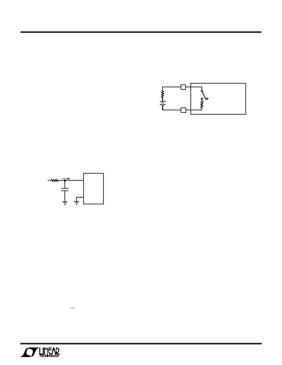
Figure 10. Reference Input Equivalent Circuit
Input Leakage Current
Input leakage currents can also create errors if the source
resistance gets too large. For instance, the maximum
input leakage specification of 1
A (at 125°C) flowing
through a source resistance of 240
will cause a voltage
drop of 240
V or 0.2LSB. This error will be much reduced
at lower temperatures because leakage drops rapidly (see
typical curve of Input Channel Leakage Current vs Tem-
perature).
REFERENCE INPUTS
The reference input of the LTC1286 is effectively a 50k
resistor from the time CS goes low to the end of the
conversion. The reference input becomes a high impedence
node at any other time (see Figure 10). Since the voltage
on the reference input defines the voltage span of the A/D
APPLICATION INFORMATION
WU
U
相关PDF资料 |
PDF描述 |
|---|---|
| LTC1327CNW#PBF | IC TXRX EIA/TIA-562 3.3V 28-DIP |
| LTC1329ACS8-50#TRPBF | IC D/A CONV 8BIT MICROPWR 8-SOIC |
| LTC1337CNW#PBF | IC 3DVR/5RCVR 5V RS232 28-DIP |
| LTC1382IN#PBF | IC TXRX 5V RS232 W/SHTDWN 18-DIP |
| LTC1383IS#TRPBF | IC TXRX 5V RS232 LOW PWR 16-SOIC |
相关代理商/技术参数 |
参数描述 |
|---|---|
| LTC1314CS | 功能描述:IC PCMCIA SWITCHNG MATRIX 14SOIC RoHS:否 类别:集成电路 (IC) >> PMIC - 电源分配开关 系列:- 特色产品:XRP252 Switches 标准包装:1 系列:- 类型:高端开关 输出数:2 Rds(开):140 毫欧 内部开关:是 电流限制:1.15A 输入电压:1.75 V ~ 5.5 V 工作温度:-40°C ~ 85°C 安装类型:表面贴装 封装/外壳:10-WFDFN 裸露焊盘 供应商设备封装:10-TDFN(3x3) 包装:Digi-Reel® 其它名称:1016-1691-6 |
| LTC1314CS#PBF | 功能描述:IC PCMCIA SWITCHNG MATRIX 14SOIC RoHS:是 类别:集成电路 (IC) >> PMIC - 电源分配开关 系列:- 特色产品:XRP252 Switches 标准包装:1 系列:- 类型:高端开关 输出数:2 Rds(开):140 毫欧 内部开关:是 电流限制:1.15A 输入电压:1.75 V ~ 5.5 V 工作温度:-40°C ~ 85°C 安装类型:表面贴装 封装/外壳:10-WFDFN 裸露焊盘 供应商设备封装:10-TDFN(3x3) 包装:Digi-Reel® 其它名称:1016-1691-6 |
| LTC1314CS#TR | 功能描述:IC SW MATRIX PCMCIA SGL 14SOIC RoHS:否 类别:集成电路 (IC) >> PMIC - 电源分配开关 系列:- 特色产品:XRP252 Switches 标准包装:1 系列:- 类型:高端开关 输出数:2 Rds(开):140 毫欧 内部开关:是 电流限制:1.15A 输入电压:1.75 V ~ 5.5 V 工作温度:-40°C ~ 85°C 安装类型:表面贴装 封装/外壳:10-WFDFN 裸露焊盘 供应商设备封装:10-TDFN(3x3) 包装:Digi-Reel® 其它名称:1016-1691-6 |
| LTC1314CS#TRPBF | 功能描述:IC PCMCIA SWITCHNG MATRIX 14SOIC RoHS:是 类别:集成电路 (IC) >> PMIC - 电源分配开关 系列:- 特色产品:XRP252 Switches 标准包装:1 系列:- 类型:高端开关 输出数:2 Rds(开):140 毫欧 内部开关:是 电流限制:1.15A 输入电压:1.75 V ~ 5.5 V 工作温度:-40°C ~ 85°C 安装类型:表面贴装 封装/外壳:10-WFDFN 裸露焊盘 供应商设备封装:10-TDFN(3x3) 包装:Digi-Reel® 其它名称:1016-1691-6 |
| LTC1315CG#PBF | 功能描述:IC PCMCIA SWITCHNG MATRIX 24SSOP RoHS:是 类别:集成电路 (IC) >> PMIC - 电源分配开关 系列:- 标准包装:80 系列:- 类型:USB 开关 输出数:2 Rds(开):135 毫欧 内部开关:是 电流限制:1.5A 输入电压:2.7 V ~ 5.5 V 工作温度:-40°C ~ 85°C 安装类型:表面贴装 封装/外壳:8-TSSOP,8-MSOP(0.118",3.00mm 宽)裸露焊盘 供应商设备封装:8-MSOP-PowerPad 包装:管件 配用:TPS2066-1EVM-296-ND - TPS2066-1EVM-296 |
发布紧急采购,3分钟左右您将得到回复。