- 您现在的位置:买卖IC网 > PDF目录10679 > LTC1407IMSE-1#PBF (Linear Technology)IC ADC 12BIT 3MSPS 10-MSOP PDF资料下载
参数资料
| 型号: | LTC1407IMSE-1#PBF |
| 厂商: | Linear Technology |
| 文件页数: | 8/26页 |
| 文件大小: | 0K |
| 描述: | IC ADC 12BIT 3MSPS 10-MSOP |
| 标准包装: | 50 |
| 位数: | 12 |
| 采样率(每秒): | 3M |
| 数据接口: | 串行,SPI? |
| 转换器数目: | 1 |
| 功率耗散(最大): | 14mW |
| 电压电源: | 单电源 |
| 工作温度: | -40°C ~ 85°C |
| 安装类型: | 表面贴装 |
| 封装/外壳: | 10-TFSOP,10-MSOP(0.118",3.00mm 宽)裸露焊盘 |
| 供应商设备封装: | 10-MSOP 裸露焊盘 |
| 包装: | 管件 |
| 输入数目和类型: | 4 个单端,单极;2 个差分,单极 |
| 产品目录页面: | 1346 (CN2011-ZH PDF) |
| 配用: | DC1082A-B-ND - BOARD SAR ADC LTC1407A DC1082A-A-ND - BOARD SAR ADC LTC1407A-1 |
LTC1407-1/LTC1407A-1
16
14071fb
APPLICATIONS INFORMATION
Board Layout and Bypassing
Wire wrap boards are not recommended for high resolu-
tion and/or high speed A/D converters. To obtain the best
performance from the LTC1407-1/LTC1407A-1, a printed
circuit board with ground plane is required. Layout for
the printed circuit board should ensure that digital and
analog signal lines are separated as much as possible. In
particular, care should be taken not to run any digital track
alongside an analog signal track. If optimum phase match
between the inputs is desired, the length of the four input
wires of the two input channels should be kept matched.
But each pair of input wires to the two input channels
should be kept separated by a ground trace to avoid high
frequency crosstalk between channels.
High quality tantalum and ceramic bypass capacitors
should be used at the VDD and VREF pins as shown in the
Block Diagram on the rst page of this data sheet. For
optimum performance, a 10μF surface mount tantalum
capacitor with a 0.1μF ceramic is recommended for the VDD
and VREF pins. Alternatively, 10μF ceramic chip capacitors
such as X5R or X7R may be used. The capacitors must be
located as close to the pins as possible. The traces con-
necting the pins and the bypass capacitors must be kept
short and should be made as wide as possible. The VDD
bypass capacitor returns to GND (Pin 6) and the VREF by-
pass capacitor returns to the Exposed Pad ground (Pin 11).
Care should be taken to place the 0.1μF VDD bypass ca-
pacitor as close to Pins 6 and 7 as possible.
Figure 7 shows the recommended system ground connec-
tions. All analog circuitry grounds should be terminated
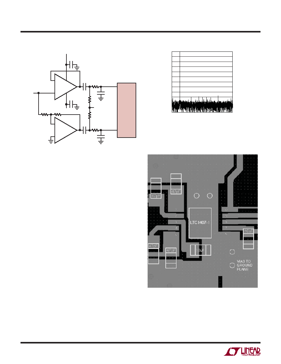
Figure 6a. The LT1819 Driving the LTC1407A-1 Differentially
Figure 6b. LTC1407-1 6MHz Sine Wave 4096 Point FFT Plot
with the LT1819 Driving the Inputs Differentially
Figure 7. Recommended Layout
–CH0 OR
–CH1
LTC1407A-1
+CH0 OR
+CH1
C1
47pF
R1
51Ω
C3
1μF
C5
0.1μF
5V
–5V
C4
1μF
R5
1k
1.5VCM
R3
499Ω
R4
499Ω
R6
1k
C2
47pF
R2
51Ω
C6
0.1μF
VIN
1.25VP-P
MAX
1407A F06a
–
+
U1
1/2 LT1819
–
+
U2
1/2 LT1819
FREQUENCY (Hz)
MAGNITUDE
(dB)
–60
–30
–20
14031 F06b
–70
–80
–120
–100
0
–10
–40
–50
–90
–110
0
371k
185k
556k
741k
1407-1 F07
相关PDF资料 |
PDF描述 |
|---|---|
| LT6700MPDCB-1#TRMPBF | IC COMP DUAL 400MV REF 6-DFN |
| VE-JWK-MY-F1 | CONVERTER MOD DC/DC 40V 50W |
| VI-B2K-MY-B1 | CONVERTER MOD DC/DC 40V 50W |
| VE-JWH-MY-F4 | CONVERTER MOD DC/DC 52V 50W |
| VI-J2Y-MY-F1 | CONVERTER MOD DC/DC 3.3V 33W |
相关代理商/技术参数 |
参数描述 |
|---|---|
| LTC1408CUH | 功能描述:IC ADC 14BIT 600KSPS 32-QFN RoHS:否 类别:集成电路 (IC) >> 数据采集 - 模数转换器 系列:- 标准包装:1,000 系列:- 位数:12 采样率(每秒):300k 数据接口:并联 转换器数目:1 功率耗散(最大):75mW 电压电源:单电源 工作温度:0°C ~ 70°C 安装类型:表面贴装 封装/外壳:24-SOIC(0.295",7.50mm 宽) 供应商设备封装:24-SOIC 包装:带卷 (TR) 输入数目和类型:1 个单端,单极;1 个单端,双极 |
| LTC1408CUH#PBF | 功能描述:IC ADC 14BIT 600KSPS 32-QFN RoHS:是 类别:集成电路 (IC) >> 数据采集 - 模数转换器 系列:- 标准包装:1 系列:microPOWER™ 位数:8 采样率(每秒):1M 数据接口:串行,SPI? 转换器数目:1 功率耗散(最大):- 电压电源:模拟和数字 工作温度:-40°C ~ 125°C 安装类型:表面贴装 封装/外壳:24-VFQFN 裸露焊盘 供应商设备封装:24-VQFN 裸露焊盘(4x4) 包装:Digi-Reel® 输入数目和类型:8 个单端,单极 产品目录页面:892 (CN2011-ZH PDF) 其它名称:296-25851-6 |
| LTC1408CUH#TRPBF | 功能描述:IC ADC 14BIT 600KSPS 32-QFN RoHS:是 类别:集成电路 (IC) >> 数据采集 - 模数转换器 系列:- 标准包装:1,000 系列:- 位数:12 采样率(每秒):300k 数据接口:并联 转换器数目:1 功率耗散(最大):75mW 电压电源:单电源 工作温度:0°C ~ 70°C 安装类型:表面贴装 封装/外壳:24-SOIC(0.295",7.50mm 宽) 供应商设备封装:24-SOIC 包装:带卷 (TR) 输入数目和类型:1 个单端,单极;1 个单端,双极 |
| LTC1408CUH-12 | 制造商:Linear Technology 功能描述:ADC Single 600ksps 12-bit Serial 32-Pin QFN EP |
| LTC1408CUH-12#PBF | 功能描述:IC ADC 12BIT 600KSPS 32-QFN RoHS:是 类别:集成电路 (IC) >> 数据采集 - 模数转换器 系列:- 标准包装:1,000 系列:- 位数:16 采样率(每秒):45k 数据接口:串行 转换器数目:2 功率耗散(最大):315mW 电压电源:模拟和数字 工作温度:0°C ~ 70°C 安装类型:表面贴装 封装/外壳:28-SOIC(0.295",7.50mm 宽) 供应商设备封装:28-SOIC W 包装:带卷 (TR) 输入数目和类型:2 个单端,单极 |
发布紧急采购,3分钟左右您将得到回复。