- 您现在的位置:买卖IC网 > PDF目录149343 > LTC1430CS#PBF (LINEAR TECHNOLOGY CORP) Isolated Flyback Switching Regulator with 9V Output PDF资料下载
参数资料
| 型号: | LTC1430CS#PBF |
| 厂商: | LINEAR TECHNOLOGY CORP |
| 元件分类: | 稳压器 |
| 英文描述: | Isolated Flyback Switching Regulator with 9V Output |
| 中文描述: | SWITCHING CONTROLLER, 500 kHz SWITCHING FREQ-MAX, PDSO16 |
| 封装: | 0.150 INCH, PLASTIC, SO-16 |
| 文件页数: | 2/16页 |
| 文件大小: | 211K |
| 代理商: | LTC1430CS#PBF |
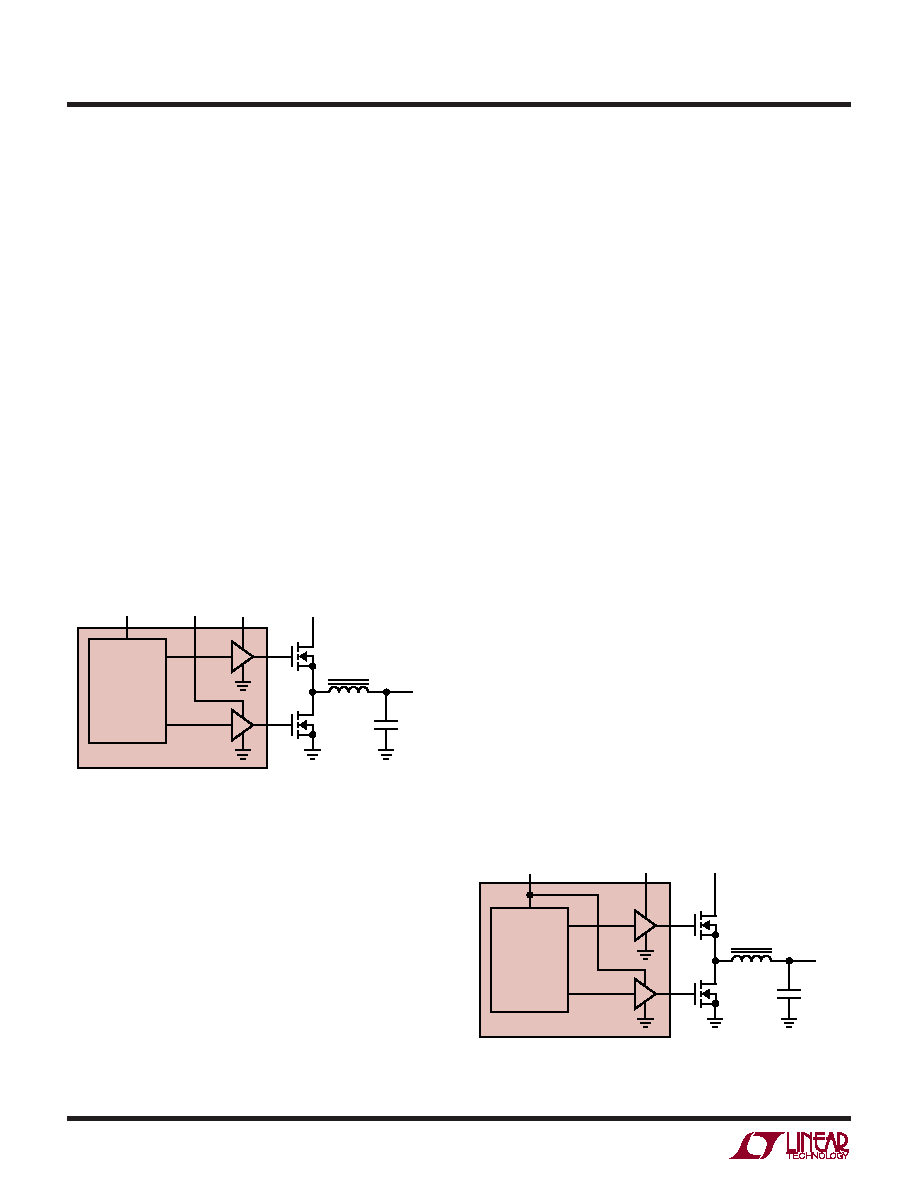
10
LTC1430
INTERNAL
CIRCUITRY
VCC/PVCC2
LTC1430 (8-LEAD)
PVCC1
M1
L1
M2
G1
G2
PVCC
COUT
VOUT
LTC1430 F07
+
Figure 7. 8-Lead Power Supplies
OS-CON part number 10SA220M (220
F/10V) capacitors
feature 2.3A allowable ripple current at 85
°C and 0.035
ESR; three in parallel at the input and six at the output will
meet the above requirements.
Input Supply Considerations/Charge Pump
The 16-lead LTC1430 requires four supply voltages to
operate: PVCC for the main power input, PVCC1 and PVCC2
for MOSFET gate drive and a clean, low ripple VCC for the
LTC1430 internal circuitry (Figure 6). In many applica-
tions, PVCC and PVCC2 can be tied together and fed from
a common high power supply, provided that the supply
voltage is high enough to fully enhance the gate of external
MOSFET M2. This can be the 5V system supply if a logic
level MOSFET is used for M2. VCC can usually be filtered
with an RC from this same high power supply; the low
quiescent current (typically 350
A) allows the use of
relatively large filter resistors and correspondingly small
filter capacitors. 100
and 4.7F usually provide ad-
equate filtering for VCC.
For both versions of the LTC1430, PVCC1 must be higher
than PVCC by at least one external MOSFET VGS(ON) to fully
enhance the gate of M1. This higher voltage can be
provided with a separate supply (typically 12V) which
should power up after PVCC, or it can be generated with a
simple charge pump (Figure 4). The charge pump consists
of a 1N4148 diode from PVCC to PVCC1 and a 0.1F
capacitor from PVCC1 to the switching node at the drain of
M2. This circuit provides 2PVCC – VF to PVCC1 while M1 is
ON and PVCC – VF while M1 is OFF where VF is the ON
voltage of the 1N4148 diode. Ringing at the drain of M2
can cause transients above 2PVCC at PVCC1; if PVCC is
higher than 7V, a 12V zener diode should be included from
PVCC1 to PGND to prevent transients from damaging the
circuitry at PVCC2 or the gate of M1.
More complex charge pumps can be constructed with the
16-lead versions of the LTC1430 to provide additional
voltages for use with standard threshold MOSFETs or very
low PVCC voltages. A tripling charge pump (Figure 5) can
provide 2PVCC and 3PVCC voltages. These can be con-
nected to PVCC2 and PVCC1 respectively, allowing stan-
dard threshold MOSFETs to be used with 5V at PVCC or 5V
logic level threshold MOSFETs to be used with 3.3V at
PVCC. VCC can be driven from the same potential as PVCC2,
allowing the entire system to run from a single 3.3V
supply. Tripling charge pumps require the use of Schottky
diodes to minimize forward drop across the diodes at
start-up. The tripling charge pump circuit will tend to
rectify any ringing at the drain of M2 and can provide well
more than 3PVCC at PVCC1; all tripling (or higher multiply-
ing factor) circuits should include a 12V zener clamp diode
DZ to prevent overvoltage at PVCC1.
INTERNAL
CIRCUITRY
VCC
LTC1430 (16-LEAD)
PVCC2
PVCC1
M1
L1
M2
G1
G2
PVCC
COUT
VOUT
LTC1430 F06
+
Figure 6. 16-Lead Power Supplies
The 8-lead versions of the LTC1430 have the PVCC2 and
VCC pins tied together inside the package (Figure 7). This
pin, brought out as VCC/PVCC2, has the same low ripple
requirements as the 16-lead part, but must also be able to
supply the gate drive current to M2. This can be obtained
by using a larger RC filter from the PVCC pin; 22 and 10F
work well here. The 10
F capacitor must be VERY close to
the part (preferably right underneath the unit) or output
regulation may suffer.
APPLICATIO S I FOR ATIO
WU
U
相关PDF资料 |
PDF描述 |
|---|---|
| LTC1430IS#PBF | Isolated Flyback Switching Regulator with 9V Output |
| LTC1430IS#TRPBF | Isolated Flyback Switching Regulator with 9V Output |
| LTC1435AIG#TRPBF | High Efficiency Low Noise Synchronous Step-Down Switching Regulator |
| LTC1435AIS#TRPBF | High Efficiency Low Noise Synchronous Step-Down Switching Regulator |
| LTC1436ACGN#PBF | RADIATION HARDENED HIGH EFFICIENCY, 5 AMP SWITCHING REGULATORS |
相关代理商/技术参数 |
参数描述 |
|---|---|
| LTC1430CSTR | 制造商:LT 功能描述:* |
| LTC1430IS | 功能描述:IC SW REG CNTRLR STEP-DWN 16SOIC RoHS:否 类别:集成电路 (IC) >> PMIC - 稳压器 - 专用型 系列:- 标准包装:43 系列:- 应用:控制器,Intel VR11 输入电压:5 V ~ 12 V 输出数:1 输出电压:0.5 V ~ 1.6 V 工作温度:-40°C ~ 85°C 安装类型:表面贴装 封装/外壳:48-VFQFN 裸露焊盘 供应商设备封装:48-QFN(7x7) 包装:管件 |
| LTC1430IS#PBF | 功能描述:IC SW REG CNTRLR STEP-DWN 16SOIC RoHS:是 类别:集成电路 (IC) >> PMIC - 稳压器 - 专用型 系列:- 标准包装:43 系列:- 应用:控制器,Intel VR11 输入电压:5 V ~ 12 V 输出数:1 输出电压:0.5 V ~ 1.6 V 工作温度:-40°C ~ 85°C 安装类型:表面贴装 封装/外壳:48-VFQFN 裸露焊盘 供应商设备封装:48-QFN(7x7) 包装:管件 |
| LTC1430IS#TR | 功能描述:IC SW REG CNTRLR STEP-DWN 16SOIC RoHS:否 类别:集成电路 (IC) >> PMIC - 稳压器 - 专用型 系列:- 标准包装:43 系列:- 应用:控制器,Intel VR11 输入电压:5 V ~ 12 V 输出数:1 输出电压:0.5 V ~ 1.6 V 工作温度:-40°C ~ 85°C 安装类型:表面贴装 封装/外壳:48-VFQFN 裸露焊盘 供应商设备封装:48-QFN(7x7) 包装:管件 |
| LTC1430IS#TRPBF | 功能描述:IC SW REG CNTRLR STEP-DWN 16SOIC RoHS:是 类别:集成电路 (IC) >> PMIC - 稳压器 - 专用型 系列:- 标准包装:43 系列:- 应用:控制器,Intel VR11 输入电压:5 V ~ 12 V 输出数:1 输出电压:0.5 V ~ 1.6 V 工作温度:-40°C ~ 85°C 安装类型:表面贴装 封装/外壳:48-VFQFN 裸露焊盘 供应商设备封装:48-QFN(7x7) 包装:管件 |
发布紧急采购,3分钟左右您将得到回复。