- 您现在的位置:买卖IC网 > PDF目录13061 > LTC1430CS#TR (Linear Technology)IC SW REG CNTRLR STEP-DWN 16SOIC PDF资料下载
参数资料
| 型号: | LTC1430CS#TR |
| 厂商: | Linear Technology |
| 文件页数: | 10/16页 |
| 文件大小: | 0K |
| 描述: | IC SW REG CNTRLR STEP-DWN 16SOIC |
| 标准包装: | 2,500 |
| 应用: | 控制器,Intel Pentium? |
| 输入电压: | 4 V ~ 8 V |
| 输出数: | 1 |
| 输出电压: | 3.3V,可调 |
| 工作温度: | 0°C ~ 70°C |
| 安装类型: | 表面贴装 |
| 封装/外壳: | 16-SOIC(0.154",3.90mm 宽) |
| 供应商设备封装: | 16-SOIC |
| 包装: | 带卷 (TR) |
�� �
�
�LTC1430�
�APPLICATIO� S� I� FOR� ATIO�
�OS-CON� part� number� 10SA220M� (220� μ� F/10V)� capacitors�
�feature� 2.3A� allowable� ripple� current� at� 85� °� C� and� 0.035� ?�
�ESR;� three� in� parallel� at� the� input� and� six� at� the� output� will�
�meet� the� above� requirements.�
�Input� Supply� Considerations/Charge� Pump�
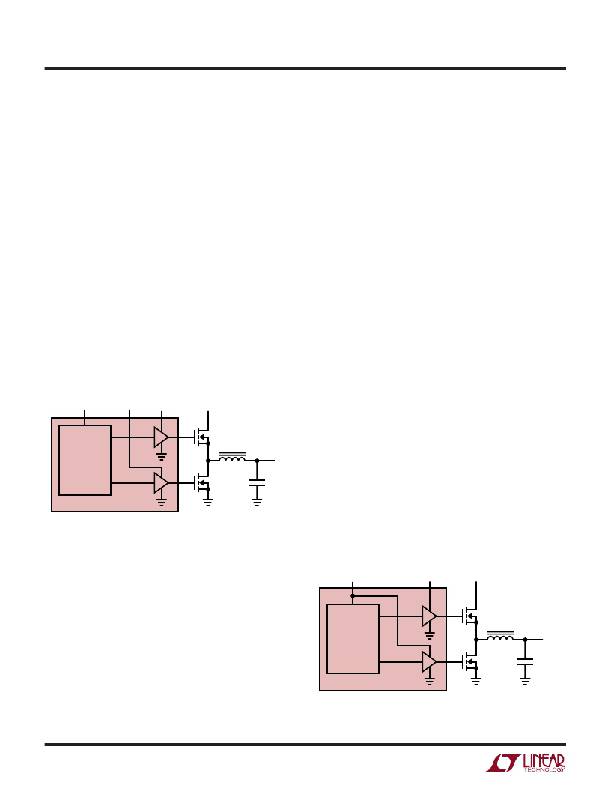
�The� 16-lead� LTC1430� requires� four� supply� voltages� to�
�operate:� PV� CC� for� the� main� power� input,� PV� CC1� and� PV� CC2�
�for� MOSFET� gate� drive� and� a� clean,� low� ripple� V� CC� for� the�
�LTC1430� internal� circuitry� (Figure� 6).� In� many� applica-�
�tions,� PV� CC� and� PV� CC2� can� be� tied� together� and� fed� from�
�a� common� high� power� supply,� provided� that� the� supply�
�voltage� is� high� enough� to� fully� enhance� the� gate� of� external�
�MOSFET� M2.� This� can� be� the� 5V� system� supply� if� a� logic�
�level� MOSFET� is� used� for� M2.� V� CC� can� usually� be� filtered�
�with� an� RC� from� this� same� high� power� supply;� the� low�
�quiescent� current� (typically� 350� μ� A)� allows� the� use� of�
�relatively� large� filter� resistors� and� correspondingly� small�
�filter� capacitors.� 100� ?� and� 4.7� μ� F� usually� provide� ad-�
�equate� filtering� for� V� CC� .�
�For� both� versions� of� the� LTC1430,� PV� CC1� must� be� higher�
�than� PV� CC� by� at� least� one� external� MOSFET� V� GS(ON)� to� fully�
�enhance� the� gate� of� M1.� This� higher� voltage� can� be�
�provided� with� a� separate� supply� (typically� 12V)� which�
�should� power� up� after� PV� CC� ,� or� it� can� be� generated� with� a�
�simple� charge� pump� (Figure� 4).� The� charge� pump� consists�
�of� a� 1N4148� diode� from� PV� CC� to� PV� CC1� and� a� 0.1� μ� F�
�capacitor� from� PV� CC1� to� the� switching� node� at� the� drain� of�
�M2.� This� circuit� provides� 2PV� CC� –� V� F� to� PV� CC1� while� M1� is�
�ON� and� PV� CC� –� V� F� while� M1� is� OFF� where� V� F� is� the� ON�
�voltage� of� the� 1N4148� diode.� Ringing� at� the� drain� of� M2�
�can� cause� transients� above� 2PV� CC� at� PV� CC1� ;� if� PV� CC� is�
�higher� than� 7V,� a� 12V� zener� diode� should� be� included� from�
�PV� CC1� to� PGND� to� prevent� transients� from� damaging� the�
�circuitry� at� PV� CC2� or� the� gate� of� M1.�
�More� complex� charge� pumps� can� be� constructed� with� the�
�16-lead� versions� of� the� LTC1430� to� provide� additional�
�voltages� for� use� with� standard� threshold� MOSFETs� or� very�
�low� PV� CC� voltages.� A� tripling� charge� pump� (Figure� 5)� can�
�provide� 2PV� CC� and� 3PV� CC� voltages.� These� can� be� con-�
�V� CC�
�PV� CC2�
�PV� CC1�
�PV� CC�
�nected� to� PV� CC2� and� PV� CC1� respectively,� allowing� stan-�
�dard� threshold� MOSFETs� to� be� used� with� 5V� at� PV� CC� or� 5V�
�INTERNAL�
�CIRCUITRY�
�G1�
�G2�
�M1�
�M2�
�L1�
�+�
�V� OUT�
�C� OUT�
�logic� level� threshold� MOSFETs� to� be� used� with� 3.3V� at�
�PV� CC� .� V� CC� can� be� driven� from� the� same� potential� as� PV� CC2� ,�
�allowing� the� entire� system� to� run� from� a� single� 3.3V�
�supply.� Tripling� charge� pumps� require� the� use� of� Schottky�
�diodes� to� minimize� forward� drop� across� the� diodes� at�
�LTC1430� (16-LEAD)�
�LTC1430� ?� F06�
�start-up.� The� tripling� charge� pump� circuit� will� tend� to�
�rectify� any� ringing� at� the� drain� of� M2� and� can� provide� well�
�Figure� 6.� 16-Lead� Power� Supplies�
�The� 8-lead� versions� of� the� LTC1430� have� the� PV� CC2� and�
�V� CC� pins� tied� together� inside� the� package� (Figure� 7).� This�
�more� than� 3PV� CC� at� PV� CC1� ;� all� tripling� (or� higher� multiply-�
�ing� factor)� circuits� should� include� a� 12V� zener� clamp� diode�
�D� Z� to� prevent� overvoltage� at� PV� CC1� .�
�pin,� brought� out� as� V� CC� /PV� CC2� ,� has� the� same� low� ripple�
�V� CC� /PV� CC2�
�PV� CC1�
�PV� CC�
�requirements� as� the� 16-lead� part,� but� must� also� be� able� to�
�supply� the� gate� drive� current� to� M2.� This� can� be� obtained�
�by� using� a� larger� RC� filter� from� the� PV� CC� pin;� 22� ?� and� 10� μ� F�
�work� well� here.� The� 10� μ� F� capacitor� must� be� VERY� close� to�
�the� part� (preferably� right� underneath� the� unit)� or� output�
�regulation� may� suffer.�
�INTERNAL�
�CIRCUITRY�
�G1�
�G2�
�M1�
�M2�
�L1�
�+�
�V� OUT�
�C� OUT�
�10�
�LTC1430� (8-LEAD)�
�Figure� 7.� 8-Lead� Power� Supplies�
�LTC1430� ?� F07�
�相关PDF资料 |
PDF描述 |
|---|---|
| MIC37300-3.3WR | IC REG LDO 3.3V 3A S-PAK-3 |
| GMA15DTAS | CONN EDGECARD 30POS R/A .125 SLD |
| LTC1736CG#TR | IC REG SW SYNC STEPDWN HE 24SSOP |
| EGM43DTKT-S288 | CONN EDGECARD 86POS .156 EXTEND |
| LTC3876EFE#TRPBF | IC CTLR DC/DC DDR DUAL 38-TSSOP |
相关代理商/技术参数 |
参数描述 |
|---|---|
| LTC1430IS | 功能描述:IC SW REG CNTRLR STEP-DWN 16SOIC RoHS:否 类别:集成电路 (IC) >> PMIC - 稳压器 - 专用型 系列:- 标准包装:43 系列:- 应用:控制器,Intel VR11 输入电压:5 V ~ 12 V 输出数:1 输出电压:0.5 V ~ 1.6 V 工作温度:-40°C ~ 85°C 安装类型:表面贴装 封装/外壳:48-VFQFN 裸露焊盘 供应商设备封装:48-QFN(7x7) 包装:管件 |
| LTC1430IS#PBF | 功能描述:IC SW REG CNTRLR STEP-DWN 16SOIC RoHS:是 类别:集成电路 (IC) >> PMIC - 稳压器 - 专用型 系列:- 标准包装:43 系列:- 应用:控制器,Intel VR11 输入电压:5 V ~ 12 V 输出数:1 输出电压:0.5 V ~ 1.6 V 工作温度:-40°C ~ 85°C 安装类型:表面贴装 封装/外壳:48-VFQFN 裸露焊盘 供应商设备封装:48-QFN(7x7) 包装:管件 |
| LTC1430IS#TR | 功能描述:IC SW REG CNTRLR STEP-DWN 16SOIC RoHS:否 类别:集成电路 (IC) >> PMIC - 稳压器 - 专用型 系列:- 标准包装:43 系列:- 应用:控制器,Intel VR11 输入电压:5 V ~ 12 V 输出数:1 输出电压:0.5 V ~ 1.6 V 工作温度:-40°C ~ 85°C 安装类型:表面贴装 封装/外壳:48-VFQFN 裸露焊盘 供应商设备封装:48-QFN(7x7) 包装:管件 |
| LTC1430IS#TRPBF | 功能描述:IC SW REG CNTRLR STEP-DWN 16SOIC RoHS:是 类别:集成电路 (IC) >> PMIC - 稳压器 - 专用型 系列:- 标准包装:43 系列:- 应用:控制器,Intel VR11 输入电压:5 V ~ 12 V 输出数:1 输出电压:0.5 V ~ 1.6 V 工作温度:-40°C ~ 85°C 安装类型:表面贴装 封装/外壳:48-VFQFN 裸露焊盘 供应商设备封装:48-QFN(7x7) 包装:管件 |
| LTC1433CGN | 功能描述:IC REG BUCK 3.3V/5V/ADJ 16SSOP RoHS:否 类别:集成电路 (IC) >> PMIC - 稳压器 - DC DC 开关稳压器 系列:- 标准包装:2,500 系列:- 类型:降压(降压) 输出类型:固定 输出数:1 输出电压:1.2V,1.5V,1.8V,2.5V 输入电压:2.7 V ~ 20 V PWM 型:- 频率 - 开关:- 电流 - 输出:50mA 同步整流器:是 工作温度:-40°C ~ 125°C 安装类型:表面贴装 封装/外壳:10-TFSOP,10-MSOP(0.118",3.00mm 宽)裸露焊盘 包装:带卷 (TR) 供应商设备封装:10-MSOP 裸露焊盘 |
发布紧急采购,3分钟左右您将得到回复。