- 您现在的位置:买卖IC网 > PDF目录15234 > LTC1438XCG#TR (Linear Technology)IC REG CTRLR BUCK PWM CM 28-SSOP PDF资料下载
参数资料
| 型号: | LTC1438XCG#TR |
| 厂商: | Linear Technology |
| 文件页数: | 16/32页 |
| 文件大小: | 0K |
| 描述: | IC REG CTRLR BUCK PWM CM 28-SSOP |
| 标准包装: | 2,000 |
| PWM 型: | 电流模式 |
| 输出数: | 2 |
| 频率 - 最大: | 138kHz |
| 占空比: | 99% |
| 电源电压: | 3.5 V ~ 30 V |
| 降压: | 是 |
| 升压: | 无 |
| 回扫: | 无 |
| 反相: | 无 |
| 倍增器: | 无 |
| 除法器: | 无 |
| Cuk: | 无 |
| 隔离: | 无 |
| 工作温度: | 0°C ~ 70°C |
| 封装/外壳: | 28-SSOP(0.209",5.30mm 宽) |
| 包装: | 带卷 (TR) |
第1页第2页第3页第4页第5页第6页第7页第8页第9页第10页第11页第12页第13页第14页第15页当前第16页第17页第18页第19页第20页第21页第22页第23页第24页第25页第26页第27页第28页第29页第30页第31页第32页
�� �
�
�LTC1438/LTC1439�
�APPLICATIO� N� S� I� N� FOR� M� ATIO� N�
�in� an� efficiency� penalty� of� up� to� 10%� at� high� input�
�voltages.�
�2.� EXTV� CC� connected� directly� to� V� OUT� .� This� is� the� normal�
�connection� for� a� 5V� regulator� and� provides� the� highest�
�efficiency.�
�3.� EXTV� CC� connected� to� an� output-derived� boost� network.�
�For� 3.3V� and� other� low� voltage� regulators,� efficiency�
�gains� can� still� be� realized� by� connecting� EXTV� CC� to� an�
�output-derived� voltage� which� has� been� boosted� to�
�greater� than� 4.8V.� This� can� be� done� with� either� the�
�inductive� boost� winding� as� shown� in� Figure� 4a� or� the�
�capacitive� charge� pump� shown� in� Figure� 4b.� The� charge�
�pump� has� the� advantage� of� simple� magnetics.�
�4.� EXTV� CC� connected� to� an� external� supply.� If� an� external�
�supply� is� available� in� the� 5V� to� 10V� range� (EXTV� CC� ≤� V� IN� )�
�it� may� be� used� to� power� EXTV� CC� providing� it� is� compat-�
�ible� with� the� MOSFET� gate� drive� requirements.� When�
�driving� standard� threshold� MOSFETs,� the� external� sup-�
�ply� must� be� always� present� during� operation� to� prevent�
�MOSFET� failure� due� to� insufficient� gate� drive.�
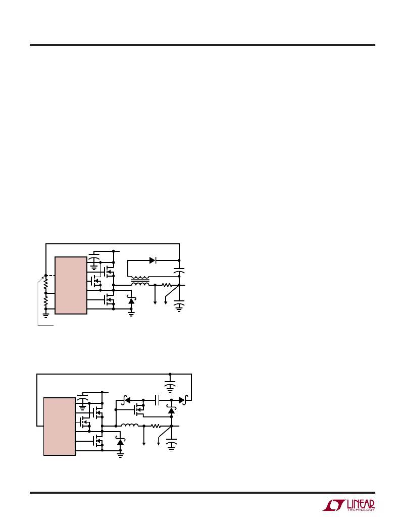
�Topside� MOSFET� Driver� Supply� (C� B� ,� D� B� )�
�External� bootstrap� capacitors� C� B� connected� to� the� BOOST�
�1� and� BOOST� 2� pins� supply� the� gate� drive� voltages� for� the�
�topside� MOSFETs.� Capacitor� C� B� in� the� Functional� Dia-�
�gram� is� charged� through� diode� D� B� from� INTV� CC� when� the�
�SW1(SW2)� pin� is� low.� When� one� of� the� topside� MOSFETs�
�is� to� be� turned� on,� the� driver� places� the� C� B� voltage� across�
�the� gate� source� of� the� desired� MOSFET.� This� enhances�
�the� MOSFET� and� turns� on� the� topside� switch.� The� switch�
�node� voltage� SW1(SW2)� rises� to� V� IN� and� the� BOOST�
�1(BOOST� 2)� pin� follows.� With� the� topside� MOSFET� on,�
�the� boost� voltage� is� above� the� input� supply:� V� BOOST� =� V� IN�
�+� V� INTVCC� .� The� value� of� the� boost� capacitor� C� B� needs� to�
�SFB1�
�R6�
�R5�
�LTC1438�
�LTC1439*�
�V� IN�
�TGL1�
�EXTV� CC�
�TGS1*�
�SW1�
�BG1�
�+�
�C� IN�
�N-CH�
�V� IN�
�N-CH�
�N-CH�
�?�
�L1�
�1:1�
�1N4148�
�?�
�V� SEC�
�+�
�R� SENSE�
�+�
�1� μ� F�
�V� OUT�
�C� OUT�
�be� 100� times� that� of� the� total� input� capacitance� of� the�
�topside� MOSFET(s).� The� reverse� breakdown� on� D� B� must�
�be� greater� than� V� IN(MAX)� .�
�Output� Voltage� Programming�
�The� LTC1438/LTC1439� have� pin� selectable� output� voltage�
�programming.� Controller� 1� on� the� LTC1438-ADJ� is� a�
�SGND�
�PGND�
�1438� F04a�
�dedicated� adjustable� controller.� The� output� voltage� is�
�OPTIONAL� EXTV� CC�
�CONNECTION�
�5V� ≤� V� SEC� ≤� 9V�
�*TGS1� ONLY� AVAILABLE� ON� THE� LTC1439�
�selected� by� the� V� PROG1� (V� PROG2� )� pin� as� follows� on� all� of� the�
�other� parts:�
�Figure� 4a.� Secondary� Output� Loop� and� EXTV� CC� Connection�
�V� PROG1,2� =� 0V�
�V� PROG1,2� =� INTV� CC�
�V� PROG2� =� Open� (DC)�
�V� OUT1,2� =� 3.3V�
�V� OUT1,2� =� 5V�
�V� OUT2� =� Adjustable�
�LTC1438�
�LTC1439*�
�V� IN�
�TGL1�
�TGS1*�
�EXTV� CC�
�SW1�
�BG1�
�PGND�
�+�
�C� IN�
�N-CH�
�V� IN�
�N-CH�
�N-CH�
�BAT85�
�L1�
�0.22� μ� F�
�VN2222LL�
�R� SENSE�
�+�
�+�
�1� μ� F�
�BAT85�
�BAT85�
�V� OUT�
�C� OUT�
�1438� F04b�
�Except� for� the� LTC1438-ADJ,� the� top� of� an� internal� resis-�
�tive� divider� is� connected� to� SENSE� –� 1� pin� in� Controller� 1.�
�For� fixed� output� voltage� applications� the� SENSE� –� 1� pin� is�
�connected� to� the� output� voltage� as� shown� in� Figure� 5a.�
�When� using� an� external� resistive� divider� for� an� adjustable�
�regulator,� the� V� PROG2� pin� is� left� open� (V� PROG1� is� internally�
�left� open� on� the� LTC1438-ADJ)� and� the� V� OSENSE2� pin� is�
�connected� to� the� feedback� resistors� as� shown� in� Figure� 5b.�
�The� adjustable� controller� will� force� the� externally� attenu-�
�*TGS1� ONLY� AVAILABLE� ON� THE� LTC1439�
�ated� output� voltage� to� 1.19V.�
�Figure� 4b.� Capacitive� Charge� Pump� for� EXTV� CC�
�14389fb�
�16�
�相关PDF资料 |
PDF描述 |
|---|---|
| VE-J7N-EY-F4 | CONVERTER MOD DC/DC 18.5V 50W |
| LTC1438XCG#PBF | IC REG CTRLR BUCK PWM CM 28-SSOP |
| VI-2TN-EW-F2 | CONVERTER MOD DC/DC 18.5V 100W |
| H2ABT-10106-B8-ND | JUMPER-H1502TR/A3048B/H1500TR 6" |
| SLPX392M050C3P3 | CAP ALUM 3900UF 50V 20% SNAP |
相关代理商/技术参数 |
参数描述 |
|---|---|
| LTC1439CG | 功能描述:IC REG CTRLR BUCK PWM CM 36-SSOP RoHS:否 类别:集成电路 (IC) >> PMIC - 稳压器 - DC DC 切换控制器 系列:- 标准包装:2,000 系列:- PWM 型:电流模式 输出数:1 频率 - 最大:1MHz 占空比:50% 电源电压:9 V ~ 10 V 降压:无 升压:是 回扫:是 反相:无 倍增器:无 除法器:无 Cuk:无 隔离:无 工作温度:-40°C ~ 85°C 封装/外壳:8-TSSOP(0.173",4.40mm 宽) 包装:带卷 (TR) |
| LTC1439CG#PBF | 功能描述:IC REG CTRLR BUCK PWM CM 36-SSOP RoHS:是 类别:集成电路 (IC) >> PMIC - 稳压器 - DC DC 切换控制器 系列:- 标准包装:2,000 系列:- PWM 型:电流模式 输出数:1 频率 - 最大:1MHz 占空比:50% 电源电压:9 V ~ 10 V 降压:无 升压:是 回扫:是 反相:无 倍增器:无 除法器:无 Cuk:无 隔离:无 工作温度:-40°C ~ 85°C 封装/外壳:8-TSSOP(0.173",4.40mm 宽) 包装:带卷 (TR) |
| LTC1439CG#TR | 功能描述:IC REG CTRLR BUCK PWM CM 36-SSOP RoHS:否 类别:集成电路 (IC) >> PMIC - 稳压器 - DC DC 切换控制器 系列:- 标准包装:4,500 系列:PowerWise® PWM 型:控制器 输出数:1 频率 - 最大:1MHz 占空比:95% 电源电压:2.8 V ~ 5.5 V 降压:是 升压:无 回扫:无 反相:无 倍增器:无 除法器:无 Cuk:无 隔离:无 工作温度:-40°C ~ 125°C 封装/外壳:6-WDFN 裸露焊盘 包装:带卷 (TR) 配用:LM1771EVAL-ND - BOARD EVALUATION LM1771 其它名称:LM1771SSDX |
| LTC1439CG#TRPBF | 功能描述:IC REG CTRLR BUCK PWM CM 36-SSOP RoHS:是 类别:集成电路 (IC) >> PMIC - 稳压器 - DC DC 切换控制器 系列:- 标准包装:4,000 系列:- PWM 型:电压模式 输出数:1 频率 - 最大:1.5MHz 占空比:66.7% 电源电压:4.75 V ~ 5.25 V 降压:是 升压:无 回扫:无 反相:无 倍增器:无 除法器:无 Cuk:无 隔离:无 工作温度:-40°C ~ 85°C 封装/外壳:40-VFQFN 裸露焊盘 包装:带卷 (TR) |
| LTC1439CGW | 功能描述:IC REG CTRLR BUCK PWM CM 36-SSOP RoHS:否 类别:集成电路 (IC) >> PMIC - 稳压器 - DC DC 切换控制器 系列:- 标准包装:4,500 系列:PowerWise® PWM 型:控制器 输出数:1 频率 - 最大:1MHz 占空比:95% 电源电压:2.8 V ~ 5.5 V 降压:是 升压:无 回扫:无 反相:无 倍增器:无 除法器:无 Cuk:无 隔离:无 工作温度:-40°C ~ 125°C 封装/外壳:6-WDFN 裸露焊盘 包装:带卷 (TR) 配用:LM1771EVAL-ND - BOARD EVALUATION LM1771 其它名称:LM1771SSDX |
发布紧急采购,3分钟左右您将得到回复。