- 您现在的位置:买卖IC网 > PDF目录15234 > LTC1438XCG#TR (Linear Technology)IC REG CTRLR BUCK PWM CM 28-SSOP PDF资料下载
参数资料
| 型号: | LTC1438XCG#TR |
| 厂商: | Linear Technology |
| 文件页数: | 17/32页 |
| 文件大小: | 0K |
| 描述: | IC REG CTRLR BUCK PWM CM 28-SSOP |
| 标准包装: | 2,000 |
| PWM 型: | 电流模式 |
| 输出数: | 2 |
| 频率 - 最大: | 138kHz |
| 占空比: | 99% |
| 电源电压: | 3.5 V ~ 30 V |
| 降压: | 是 |
| 升压: | 无 |
| 回扫: | 无 |
| 反相: | 无 |
| 倍增器: | 无 |
| 除法器: | 无 |
| Cuk: | 无 |
| 隔离: | 无 |
| 工作温度: | 0°C ~ 70°C |
| 封装/外壳: | 28-SSOP(0.209",5.30mm 宽) |
| 包装: | 带卷 (TR) |
第1页第2页第3页第4页第5页第6页第7页第8页第9页第10页第11页第12页第13页第14页第15页第16页当前第17页第18页第19页第20页第21页第22页第23页第24页第25页第26页第27页第28页第29页第30页第31页第32页
�� �
�
�LTC1438/LTC1439�
�APPLICATIO� N� S� I� N� FOR� M� ATIO� N�
�SENSE� 1�
�V� PROG1�
�–�
�LTC1438�
�LTC1439�
�SGND�
�GND:� V� OUT� =� 3.3V�
�INTV� CC� :� V� OUT� =� 5V�
�+�
�V� OUT�
�C� OUT�
�1438� F05a�
�the� internal� current� limit.� Power� supply� sequencing� can�
�also� be� accomplished� using� this� pin.�
�An� internal� 3� μ� A� current� source� charges� up� an� external�
�capacitor� C� SS.� When� the� voltage� on� RUN/SS1� (RUN/SS2)�
�reaches� 1.3V� the� particular� controller� is� permitted� to� start�
�Figure� 5a.� LTC1438/LTC1439� Fixed� Output� Applications�
�1.19V� ≤� V� OUT� ≤� 9V�
�operating.� As� the� voltage� on� the� pin� continues� to� ramp�
�from� 1.3V� to� 2.4V,� the� internal� current� limit� is� also� ramped�
�at� a� proportional� linear� rate.� The� current� limit� begins� at�
�V� PROG2� *�
�V� OSENSE1,2�
�LTC1438�
�LTC1439�
�OPEN� (DC)�
�100pF�
�R2�
�R1�
�approximately� 50mV/R� SENSE� (at� V� RUN/SS� =� 1.3V)� and� ends�
�at� 150mV/R� SENSE� (V� RUN/SS� ≥� 2.7V).� The� output� current�
�thus� ramps� up� slowly,� reducing� the� starting� surge� current�
�required� from� the� input� power� supply.� If� RUN/SS� has� been�
�(� )�
�V� OUT� =� 1.19V� 1� +�
�SGND�
�*LTC1439� ONLY�
�R2�
�R1�
�1438� F05b�
�pulled� all� the� way� to� ground� there� is� a� delay� before� starting�
�of� approximately� 500ms/� μ� F,� followed� by� a� similar� time� to�
�reach� full� current� on� that� controller.�
�Figure� 5b.� LTC1438/LTC1439� Adjustable� Applications�
�Power-On� Reset� Function� (POR)�
�The� power-on� reset� function� (not� available� on� the�
�LTC1438X)� monitors� the� output� voltage� of� the� second�
�controller� and� turns� on� an� open� drain� device� when� it� is�
�below� its� properly� regulated� voltage.� An� external� pull-up�
�resistor� is� required� on� the� POR2� pin.�
�By� pulling� both� RUN/SS� controller� pins� below� 1.3V,� the�
�LTC1438/LTC1439� are� put� into� low� current� shutdown�
�(I� Q� <� 25� μ� A).� These� pins� can� be� driven� directly� from� logic� as�
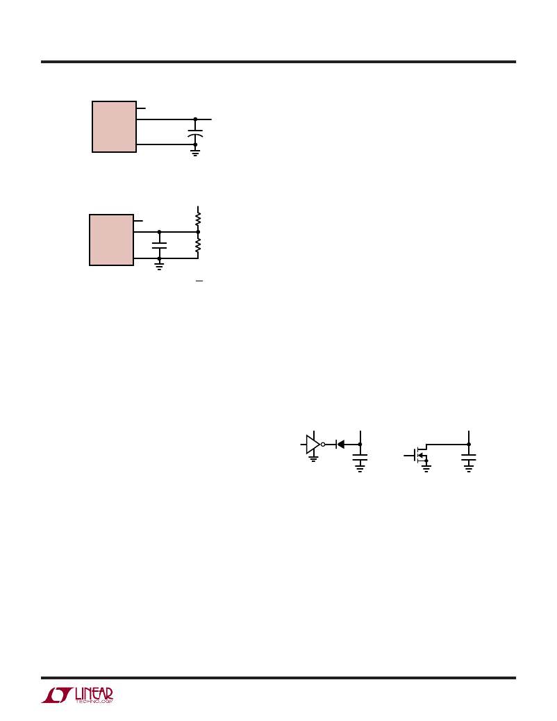
�shown� in� Figure� 6.� Diode� D1� in� Figure� 6� reduces� the� start�
�delay� but� allows� C� SS� to� ramp� up� slowly� providing� the� soft�
�start� function;� this� diode� and� C� SS� can� be� deleted� if� soft� start�
�is� not� needed.� Each� RUN/SS� pin� has� an� internal� 6V� Zener�
�clamp� (See� Functional� Diagram).�
�When� power� is� first� applied� or� when� coming� out� of�
�shutdown,� the� POR2� output� is� held� at� ground.� When� the�
�output� voltage� rises� above� a� level� which� is� 5%� below� the�
�3.3V�
�OR� 5V�
�D1�
�RUN/SS1�
�(RUN/SS2)�
�RUN/SS1�
�(RUN/SS2)�
�final� regulated� output� value,� an� internal� counter� starts.�
�After� this� counter� counts� 2� 16� (65536)� clock� cycles,� the�
�POR2� pull-down� device� turns� off.�
�The� POR2� output� will� go� low� whenever� the� output� voltage�
�C� SS�
�Figure� 6.� RUN/SS� Pin� Interfacing�
�C� SS�
�1438� F06�
�of� the� second� controller� drops� below� 7.5%� of� its� regulated�
�value� for� longer� than� approximately� 30� μ� s,� signaling� an�
�out-of-regulation� condition.� In� shutdown,� when� RUN/SS1�
�and� RUN/SS2� are� both� below� 1.3V,� the� POR2� output� is�
�pulled� low� even� if� the� regulator’s� output� is� held� up� by� an�
�external� source.� The� POR2� output� is� active� during� shut-�
�down� if� V� IN� is� powered.�
�Run/� Soft� Start� Function�
�The� RUN/SS1� and� RUN/SS2� pins� each� serve� two� func-�
�tions.� Each� pin� provides� the� soft� start� function� and� a�
�means� to� shut� down� each� controller.� Soft� start� reduces�
�surge� currents� from� V� IN� by� providing� a� gradual� ramp-up� of�
�Foldback� Current� Limiting�
�As� described� in� Power� MOSFET� and� D1� Selection,� the�
�worst-case� dissipation� for� either� MOSFET� occurs� with� a�
�short-circuited� output,� when� the� synchronous� MOSFET�
�conducts� the� current� limit� value� almost� continuously.� In�
�most� applications� this� will� not� cause� excessive� heating,�
�even� for� extended� fault� intervals.� However,� when� heat�
�sinking� is� at� a� premium� or� higher� R� DS(ON)� MOSFETs� are�
�being� used,� foldback� current� limiting� should� be� added� to�
�reduce� the� current� in� proportion� to� the� severity� of� the� fault.�
�Foldback� current� limiting� is� implemented� by� adding� diode�
�D� FB� between� the� output� and� the� I� TH� pin� as� shown� in� the�
�14389fb�
�17�
�相关PDF资料 |
PDF描述 |
|---|---|
| VE-J7N-EY-F4 | CONVERTER MOD DC/DC 18.5V 50W |
| LTC1438XCG#PBF | IC REG CTRLR BUCK PWM CM 28-SSOP |
| VI-2TN-EW-F2 | CONVERTER MOD DC/DC 18.5V 100W |
| H2ABT-10106-B8-ND | JUMPER-H1502TR/A3048B/H1500TR 6" |
| SLPX392M050C3P3 | CAP ALUM 3900UF 50V 20% SNAP |
相关代理商/技术参数 |
参数描述 |
|---|---|
| LTC1439CG | 功能描述:IC REG CTRLR BUCK PWM CM 36-SSOP RoHS:否 类别:集成电路 (IC) >> PMIC - 稳压器 - DC DC 切换控制器 系列:- 标准包装:2,000 系列:- PWM 型:电流模式 输出数:1 频率 - 最大:1MHz 占空比:50% 电源电压:9 V ~ 10 V 降压:无 升压:是 回扫:是 反相:无 倍增器:无 除法器:无 Cuk:无 隔离:无 工作温度:-40°C ~ 85°C 封装/外壳:8-TSSOP(0.173",4.40mm 宽) 包装:带卷 (TR) |
| LTC1439CG#PBF | 功能描述:IC REG CTRLR BUCK PWM CM 36-SSOP RoHS:是 类别:集成电路 (IC) >> PMIC - 稳压器 - DC DC 切换控制器 系列:- 标准包装:2,000 系列:- PWM 型:电流模式 输出数:1 频率 - 最大:1MHz 占空比:50% 电源电压:9 V ~ 10 V 降压:无 升压:是 回扫:是 反相:无 倍增器:无 除法器:无 Cuk:无 隔离:无 工作温度:-40°C ~ 85°C 封装/外壳:8-TSSOP(0.173",4.40mm 宽) 包装:带卷 (TR) |
| LTC1439CG#TR | 功能描述:IC REG CTRLR BUCK PWM CM 36-SSOP RoHS:否 类别:集成电路 (IC) >> PMIC - 稳压器 - DC DC 切换控制器 系列:- 标准包装:4,500 系列:PowerWise® PWM 型:控制器 输出数:1 频率 - 最大:1MHz 占空比:95% 电源电压:2.8 V ~ 5.5 V 降压:是 升压:无 回扫:无 反相:无 倍增器:无 除法器:无 Cuk:无 隔离:无 工作温度:-40°C ~ 125°C 封装/外壳:6-WDFN 裸露焊盘 包装:带卷 (TR) 配用:LM1771EVAL-ND - BOARD EVALUATION LM1771 其它名称:LM1771SSDX |
| LTC1439CG#TRPBF | 功能描述:IC REG CTRLR BUCK PWM CM 36-SSOP RoHS:是 类别:集成电路 (IC) >> PMIC - 稳压器 - DC DC 切换控制器 系列:- 标准包装:4,000 系列:- PWM 型:电压模式 输出数:1 频率 - 最大:1.5MHz 占空比:66.7% 电源电压:4.75 V ~ 5.25 V 降压:是 升压:无 回扫:无 反相:无 倍增器:无 除法器:无 Cuk:无 隔离:无 工作温度:-40°C ~ 85°C 封装/外壳:40-VFQFN 裸露焊盘 包装:带卷 (TR) |
| LTC1439CGW | 功能描述:IC REG CTRLR BUCK PWM CM 36-SSOP RoHS:否 类别:集成电路 (IC) >> PMIC - 稳压器 - DC DC 切换控制器 系列:- 标准包装:4,500 系列:PowerWise® PWM 型:控制器 输出数:1 频率 - 最大:1MHz 占空比:95% 电源电压:2.8 V ~ 5.5 V 降压:是 升压:无 回扫:无 反相:无 倍增器:无 除法器:无 Cuk:无 隔离:无 工作温度:-40°C ~ 125°C 封装/外壳:6-WDFN 裸露焊盘 包装:带卷 (TR) 配用:LM1771EVAL-ND - BOARD EVALUATION LM1771 其它名称:LM1771SSDX |
发布紧急采购,3分钟左右您将得到回复。