- 您现在的位置:买卖IC网 > PDF目录10092 > LTC1604CG#TRPBF (Linear Technology)IC A/D CONV 16BIT SAMPLNG 36SSOP PDF资料下载
参数资料
| 型号: | LTC1604CG#TRPBF |
| 厂商: | Linear Technology |
| 文件页数: | 19/20页 |
| 文件大小: | 0K |
| 描述: | IC A/D CONV 16BIT SAMPLNG 36SSOP |
| 标准包装: | 2,000 |
| 位数: | 16 |
| 采样率(每秒): | 333k |
| 数据接口: | 并联 |
| 转换器数目: | 1 |
| 功率耗散(最大): | 350mW |
| 电压电源: | 双 ± |
| 工作温度: | 0°C ~ 70°C |
| 安装类型: | 表面贴装 |
| 封装/外壳: | 36-SSOP(0.209",5.30mm 宽) |
| 供应商设备封装: | 36-SSOP |
| 包装: | 带卷 (TR) |
| 输入数目和类型: | 2 个单端,双极;1 个差分,双极 |
LTC1604
8
1604fa
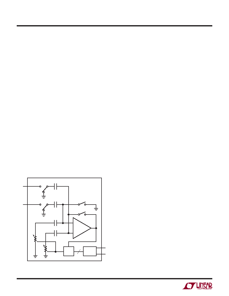
CONVERSION DETAILS
The LTC1604 uses a successive approximation algorithm
and internal sample-and-hold circuit to convert an analog
signal to a 16-bit parallel output. The ADC is complete with
a sample-and-hold, a precision reference and an internal
clock. The control logic provides easy interface to micro-
processors and DSPs. (Please refer to the Digital Interface
section for the data format.)
Conversion start is controlled by the CS and CONVST
inputs. At the start of the conversion the successive
approximation register (SAR) resets. Once a conversion
cycle has begun it cannot be restarted.
During the conversion, the internal differential 16-bit
capacitive DAC output is sequenced by the SAR from the
Most Significant Bit (MSB) to the Least Significant Bit
(LSB). Referring to Figure 1, the AIN+ and AIN– inputs are
acquired during the acquire phase and the comparator
offset is nulled by the zeroing switches. In this acquire
phase, a duration of 480ns will provide enough time for the
sample-and-hold capacitors to acquire the analog signal.
During the convert phase the comparator zeroing switches
open, putting the comparator into compare mode. The
input switches connect the CSMPL capacitors to ground,
transferring the differential analog input charge onto the
APPLICATIONS INFORMATION
summing junctions. This input charge is successively
compared with the binary-weighted charges supplied by
the differential capacitive DAC. Bit decisions are made by
the high speed comparator. At the end of a conversion, the
differential DAC output balances the AIN+ and AIN– input
charges. The SAR contents (a 16-bit data word) which
represent the difference of AIN+ and AIN– are loaded into
the 16-bit output latches.
DIGITAL INTERFACE
The A/D converter is designed to interface with micropro-
cessors as a memory mapped device. The CS and RD
control inputs are common to all peripheral memory
interfacing. A separate CONVST is used to initiate a con-
version.
Internal Clock
The A/D converter has an internal clock that runs the A/D
conversion. The internal clock is factory trimmed to achieve
a typical conversion time of 2.45μs and a maximum
conversion time of 2.8μs over the full temperature range.
No external adjustments are required. The guaranteed
maximum acquisition time is 480ns. In addition, a through-
put time (acquisition + conversion) of 3μs and a minimum
sampling rate of 333ksps are guaranteed.
3V Input/Output Compatible
The LTC1604 operates on ±5V supplies, which makes the
device easy to interface to 5V digital systems. This device
can also talk to 3V digital systems: the digital input pins
(SHDN, CS, CONVST and RD) of the LTC1604 recognize
3V or 5V inputs. The LTC1604 has a dedicated output
supply pin (OVDD) that controls the output swings of the
digital output pins (D0 to D15, BUSY) and allows the part
to talk to either 3V or 5V digital systems. The output is
two’s complement binary.
Power Shutdown
The LTC1604 provides two power shutdown modes, Nap
and Sleep, to save power during inactive periods. The
Nap mode reduces the power by 95% and leaves only the
digital logic and reference powered up. The wake-up
time from Nap to active is 200ns. In Sleep mode all bias
Figure 1. Simplified Block Diagram
–
+
COMP
AIN
+
CSMPL
HOLD
SAMPLE
AIN
–
CSMPL
+CDAC
+VDAC
–CDAC
–VDAC
HOLD
SAMPLE
HOLD
SAR
OUTPUT
LATCHES
16
D15
D0
1604 F01
ZEROING SWITCHES
相关PDF资料 |
PDF描述 |
|---|---|
| IDT72215LB15PFI8 | IC FIFO 512X18 SYNC 15NS 64-TQFP |
| VI-2TY-MX | CONVERTER MOD DC/DC 3.3V 49.5W |
| MS27474E12F35SB | CONN RCPT 22POS JAM NUT W/SCKT |
| MS3102R16S-3P | CONN RCPT 1POS BOX MNT W/PINS |
| LTC1480IS8 | IC TXRX 3.3V RS485 LOWPWR 8-SOIC |
相关代理商/技术参数 |
参数描述 |
|---|---|
| LTC1604IG | 功能描述:IC A/D CONV 16BIT SAMPLNG 36SSOP RoHS:否 类别:集成电路 (IC) >> 数据采集 - 模数转换器 系列:- 标准包装:1 系列:- 位数:14 采样率(每秒):83k 数据接口:串行,并联 转换器数目:1 功率耗散(最大):95mW 电压电源:双 ± 工作温度:0°C ~ 70°C 安装类型:通孔 封装/外壳:28-DIP(0.600",15.24mm) 供应商设备封装:28-PDIP 包装:管件 输入数目和类型:1 个单端,双极 |
| LTC1604IG#PBF | 功能描述:IC A/D CONV 16BIT SAMPLNG 36SSOP RoHS:是 类别:集成电路 (IC) >> 数据采集 - 模数转换器 系列:- 标准包装:1 系列:- 位数:14 采样率(每秒):83k 数据接口:串行,并联 转换器数目:1 功率耗散(最大):95mW 电压电源:双 ± 工作温度:0°C ~ 70°C 安装类型:通孔 封装/外壳:28-DIP(0.600",15.24mm) 供应商设备封装:28-PDIP 包装:管件 输入数目和类型:1 个单端,双极 |
| LTC1604IG#TR | 功能描述:IC ADC 16BIT SAMPL SHTDWN 36SSOP RoHS:否 类别:集成电路 (IC) >> 数据采集 - 模数转换器 系列:- 标准包装:1 系列:- 位数:14 采样率(每秒):83k 数据接口:串行,并联 转换器数目:1 功率耗散(最大):95mW 电压电源:双 ± 工作温度:0°C ~ 70°C 安装类型:通孔 封装/外壳:28-DIP(0.600",15.24mm) 供应商设备封装:28-PDIP 包装:管件 输入数目和类型:1 个单端,双极 |
| LTC1604IG#TRPBF | 功能描述:IC A/D CONV 16BIT SAMPLNG 36SSOP RoHS:是 类别:集成电路 (IC) >> 数据采集 - 模数转换器 系列:- 标准包装:1 系列:- 位数:14 采样率(每秒):83k 数据接口:串行,并联 转换器数目:1 功率耗散(最大):95mW 电压电源:双 ± 工作温度:0°C ~ 70°C 安装类型:通孔 封装/外壳:28-DIP(0.600",15.24mm) 供应商设备封装:28-PDIP 包装:管件 输入数目和类型:1 个单端,双极 |
| LTC1605-1CG | 功能描述:IC A/D CONV 16BIT SAMPLNG 28SSOP RoHS:否 类别:集成电路 (IC) >> 数据采集 - 模数转换器 系列:- 标准包装:1,000 系列:- 位数:12 采样率(每秒):300k 数据接口:并联 转换器数目:1 功率耗散(最大):75mW 电压电源:单电源 工作温度:0°C ~ 70°C 安装类型:表面贴装 封装/外壳:24-SOIC(0.295",7.50mm 宽) 供应商设备封装:24-SOIC 包装:带卷 (TR) 输入数目和类型:1 个单端,单极;1 个单端,双极 |
发布紧急采购,3分钟左右您将得到回复。