- 您现在的位置:买卖IC网 > PDF目录15503 > LTC1622IS8#PBF (Linear Technology)IC REG CTRLR BUCK PWM CM 8-SOIC PDF资料下载
参数资料
| 型号: | LTC1622IS8#PBF |
| 厂商: | Linear Technology |
| 文件页数: | 10/16页 |
| 文件大小: | 0K |
| 描述: | IC REG CTRLR BUCK PWM CM 8-SOIC |
| 标准包装: | 100 |
| PWM 型: | 电流模式 |
| 输出数: | 1 |
| 频率 - 最大: | 625kHz |
| 占空比: | 100% |
| 电源电压: | 2 V ~ 10 V |
| 降压: | 是 |
| 升压: | 无 |
| 回扫: | 无 |
| 反相: | 无 |
| 倍增器: | 无 |
| 除法器: | 无 |
| Cuk: | 无 |
| 隔离: | 无 |
| 工作温度: | -45°C ~ 85°C |
| 封装/外壳: | 8-SOIC(0.154",3.90mm 宽) |
| 包装: | 管件 |
�� �
�
�LTC1622�
�APPLICATIO� N� S� I� N� FOR� M� ATIO� N�
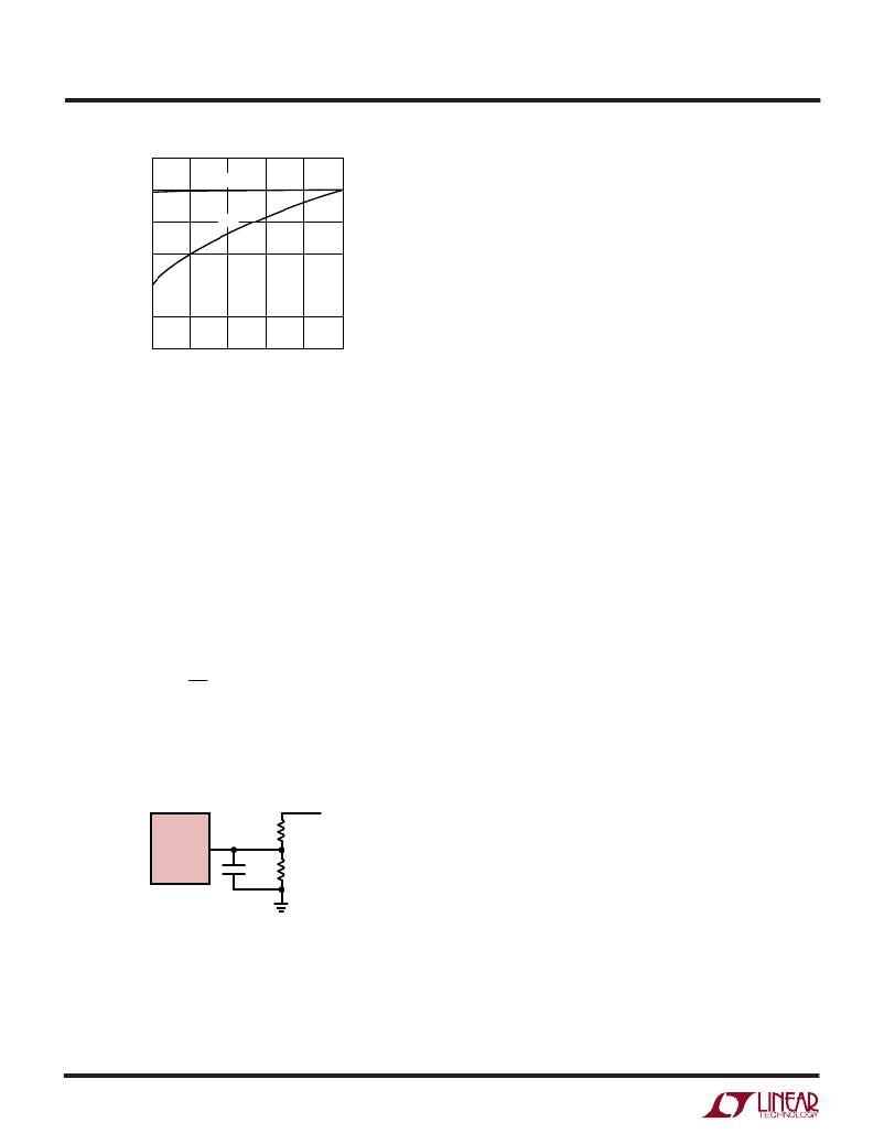
�101�
�is� limiting� the� efficiency� and� which� change� would� produce�
�100�
�99�
�98�
�97�
�96�
�V� REF�
�V� ITH�
�the� most� improvement.� Efficiency� can� be� expressed� as:�
�Efficiency� =� 100%� –� (� η� 1� +� η� 2� +� η� 3� +� ...)�
�where� η� 1,� η� 2,� etc.� are� the� individual� losses� as� a� percent-�
�age� of� input� power.�
�Although� all� dissipative� elements� in� the� circuit� produce�
�losses,� four� main� sources� usually� account� for� most� of� the�
�losses� in� LTC1622� circuits:� 1)� LTC1622� DC� bias� current,�
�95�
�2.0�
�2.2�
�2.4� 2.6� 2.8�
�3.0�
�2)� MOSFET� gate� charge� current,� 3)� I� 2� R� losses,� 4)� voltage�
�INPUT� VOLTAGE� (V)�
�1622� F03�
�drop� of� the� output� diode� and� 5)� transition� losses.�
�Figure� 3.� Line� Regulation� of� V� REF� and� V� ITH�
�the� maximum� current� sense� voltage� that� sets� the� maxi-�
�mum� output� current.�
�Setting� Output� Voltage�
�The� LTC1622� develops� a� 0.8V� reference� voltage� between�
�the� feedback� (Pin� 3)� terminal� and� ground� (see� Figure� 4).� By�
�selecting� resistor� R1,� a� constant� current� is� caused� to� flow�
�through� R1� and� R2� to� set� the� output� voltage.� The� regulated�
�output� voltage� is� determined� by:�
�1.� The� V� IN� current� is� the� DC� supply� current,� given� in� the�
�electrical� characteristics,� that� excludes� MOSFET� driver�
�and� control� currents.� V� IN� current� results� in� a� small� loss�
�which� increases� with� V� IN� .�
�2.� MOSFET� gate� charge� current� results� from� switching�
�the� gate� capacitance� of� the� power� MOSFET.� Each� time�
�a� MOSFET� gate� is� switched� from� low� to� high� to� low�
�again,� a� packet� of� charge� dQ� moves� from� V� IN� to� ground.�
�The� resulting� dQ/dt� is� a� current� out� of� V� IN� which� is�
�typically� much� larger� than� the� DC� supply� current.� In�
�continuous� mode,� I� GATECHG� =� f(Qp).�
�V� OUT� =� 0� .� 8� ?� 1� +�
�?�
�?�
�R� 2� ?�
�R� 1� ?� ?�
�3.� I� 2� R� losses� are� predicted� from� the� DC� resistances� of� the�
�MOSFET,� inductor� and� current� shunt.� In� continuous�
�mode� the� average� output� current� flows� through� L� but�
�For� most� applications,� a� 30k� resistor� is� suggested� for� R1.�
�To� prevent� stray� pickup,� an� optional� 100pF� capacitor� is�
�suggested� across� R1� located� close� to� LTC1622.�
�is� “chopped”� between� the� P-channel� MOSFET� in� series�
�with� R� SENSE� and� the� output� diode.� The� MOSFET� R� DS(ON)�
�plus� R� SENSE� multiplied� by� duty� cycle� can� be� summed�
�with� the� resistance� of� the� inductor� to� obtain� I� 2� R� losses.�
�LTC1622�
�V� FB�
�3�
�100pF�
�R2�
�R1�
�V� OUT�
�4.� The� output� diode� is� a� major� source� of� power� loss� at�
�high� currents� and� gets� worse� at� high� input� voltages.�
�The� diode� loss� is� calculated� by� multiplying� the� forward�
�voltage� drop� times� the� diode� duty� cycle� multiplied� by�
�the� load� current.� For� example,� assuming� a� duty� cycle� of�
�1622� F04�
�Figure� 4.� Setting� Output� Voltage�
�Efficiency� Considerations�
�The� efficiency� of� a� switching� regulator� is� equal� to� the�
�output� power� divided� by� the� input� power� times� 100%.� It� is�
�often� useful� to� analyze� individual� losses� to� determine� what�
�10�
�50%� with� a� Schottky� diode� forward� voltage� drop� of�
�0.4V,� the� loss� increases� from� 0.5%� to� 8%� as� the� load�
�current� increases� from� 0.5A� to� 2A.�
�5.� Transition� losses� apply� to� the� external� MOSFET� and�
�increase� with� higher� operating� frequencies� and� input�
�voltages.� Transition� losses� can� be� estimated� from:�
�相关PDF资料 |
PDF描述 |
|---|---|
| MIC2182-5.0YSM | IC REG CTRLR BUCK PWM CM 16-SSOP |
| SPD62-352M | INDUCTOR PWR SHIELDED 3.50UH SMD |
| SPD62-242M | INDUCTOR PWR SHIELDED 2.40UH SMD |
| URZ0J332MHD | CAP ALUM 3300UF 6.3V 20% RADIAL |
| UPM1A122MHD6 | CAP ALUM 1200UF 10V 20% RADIAL |
相关代理商/技术参数 |
参数描述 |
|---|---|
| LTC1623CMS8 | 功能描述:IC HI-SIDE SW CNTRLR DUAL 8-MSOP RoHS:否 类别:集成电路 (IC) >> PMIC - MOSFET,电桥驱动器 - 外部开关 系列:- 标准包装:5 系列:- 配置:低端 输入类型:非反相 延迟时间:600ns 电流 - 峰:12A 配置数:1 输出数:1 高端电压 - 最大(自引导启动):- 电源电压:14.2 V ~ 15.8 V 工作温度:-20°C ~ 60°C 安装类型:通孔 封装/外壳:21-SIP 模块 供应商设备封装:模块 包装:散装 配用:BG2A-NF-ND - KIT DEV BOARD FOR IGBT 其它名称:835-1063 |
| LTC1623CMS8#PBF | 功能描述:IC HI-SIDE SW CNTRLR DUAL 8-MSOP RoHS:是 类别:集成电路 (IC) >> PMIC - MOSFET,电桥驱动器 - 外部开关 系列:- 标准包装:50 系列:- 配置:高端 输入类型:非反相 延迟时间:200ns 电流 - 峰:250mA 配置数:1 输出数:1 高端电压 - 最大(自引导启动):600V 电源电压:12 V ~ 20 V 工作温度:-40°C ~ 125°C 安装类型:通孔 封装/外壳:8-DIP(0.300",7.62mm) 供应商设备封装:8-DIP 包装:管件 其它名称:*IR2127 |
| LTC1623CMS8#TR | 功能描述:IC CTRLR SW SMBUS DUAL 8MSOP RoHS:否 类别:集成电路 (IC) >> PMIC - MOSFET,电桥驱动器 - 外部开关 系列:- 标准包装:5 系列:- 配置:低端 输入类型:非反相 延迟时间:600ns 电流 - 峰:12A 配置数:1 输出数:1 高端电压 - 最大(自引导启动):- 电源电压:14.2 V ~ 15.8 V 工作温度:-20°C ~ 60°C 安装类型:通孔 封装/外壳:21-SIP 模块 供应商设备封装:模块 包装:散装 配用:BG2A-NF-ND - KIT DEV BOARD FOR IGBT 其它名称:835-1063 |
| LTC1623CMS8#TRPBF | 功能描述:IC HI-SIDE SW CNTRLR DUAL 8-MSOP RoHS:是 类别:集成电路 (IC) >> PMIC - MOSFET,电桥驱动器 - 外部开关 系列:- 标准包装:50 系列:- 配置:高端 输入类型:非反相 延迟时间:200ns 电流 - 峰:250mA 配置数:1 输出数:1 高端电压 - 最大(自引导启动):600V 电源电压:12 V ~ 20 V 工作温度:-40°C ~ 125°C 安装类型:通孔 封装/外壳:8-DIP(0.300",7.62mm) 供应商设备封装:8-DIP 包装:管件 其它名称:*IR2127 |
| LTC1623CS8 | 功能描述:IC HI-SIDE SW CNTRLR DUAL 8-SOIC RoHS:否 类别:集成电路 (IC) >> PMIC - MOSFET,电桥驱动器 - 外部开关 系列:- 标准包装:5 系列:- 配置:低端 输入类型:非反相 延迟时间:600ns 电流 - 峰:12A 配置数:1 输出数:1 高端电压 - 最大(自引导启动):- 电源电压:14.2 V ~ 15.8 V 工作温度:-20°C ~ 60°C 安装类型:通孔 封装/外壳:21-SIP 模块 供应商设备封装:模块 包装:散装 配用:BG2A-NF-ND - KIT DEV BOARD FOR IGBT 其它名称:835-1063 |
发布紧急采购,3分钟左右您将得到回复。