- 您现在的位置:买卖IC网 > PDF目录15503 > LTC1622IS8#PBF (Linear Technology)IC REG CTRLR BUCK PWM CM 8-SOIC PDF资料下载
参数资料
| 型号: | LTC1622IS8#PBF |
| 厂商: | Linear Technology |
| 文件页数: | 12/16页 |
| 文件大小: | 0K |
| 描述: | IC REG CTRLR BUCK PWM CM 8-SOIC |
| 标准包装: | 100 |
| PWM 型: | 电流模式 |
| 输出数: | 1 |
| 频率 - 最大: | 625kHz |
| 占空比: | 100% |
| 电源电压: | 2 V ~ 10 V |
| 降压: | 是 |
| 升压: | 无 |
| 回扫: | 无 |
| 反相: | 无 |
| 倍增器: | 无 |
| 除法器: | 无 |
| Cuk: | 无 |
| 隔离: | 无 |
| 工作温度: | -45°C ~ 85°C |
| 封装/外壳: | 8-SOIC(0.154",3.90mm 宽) |
| 包装: | 管件 |
�� �
�
�LTC1622�
�APPLICATIO� N� S� I� N� FOR� M� ATIO� N�
�R� DS� (� ON� )� ?�
�=� 0� .� 11� ?�
�(� )� (� )� p� δ�
�1� +�
�down to 2.7V. Let’s assume that the MOSFET dissipation�
�is� to� be� limited� to� P� P� =� 250mW� and� its� thermal� resistance�
�is� 50� °� C/W.� Hence� the� junction� temperature� at� T� A� =� 25� °� C�
�will� be� 37.5� °� C� and� δ� p� =� 0.005� (37.5� –� 25)� =� 0.0625.� The�
�required� R� DS(ON)� is� then� given� by:�
�P� P�
�2�
�DC� I� OUT�
�The� P-channel� MOSFET� requirement� can� be� met� by� an�
�Si6433DQ.�
�The� requirement� for� the� Schottky� diode� is� the� most� strin-�
�gent� when� V� OUT� =� 0V,� i.e.,� short� circuit.� With� a� 0.025� ?�
�R� SENSE� resistor,� the� short-circuit� current� through� the�
�Schottky� is� 0.1/0.025� =� 4A.� An� MBRS340T3� Schottky�
�diode� is� chosen.� With� 4A� flowing� through,� the� diode� is�
�rated� with� a� forward� voltage� of� 0.4V.� Therefore,� the� worst-�
�case� power� dissipated� by� the� diode� is� 1.6W.� The� addition�
�of� D� FB� (Figure� 5)� will� reduce� the� diode� dissipation� to�
�approximately� 0.8W.�
�The� input� capacitor� requires� an� RMS� current� rating� of� at�
�least� 0.75A� at� temperature,� and� C� OUT� will� require� an� ESR�
�of� 0.1� ?� for� optimum� efficiency.�
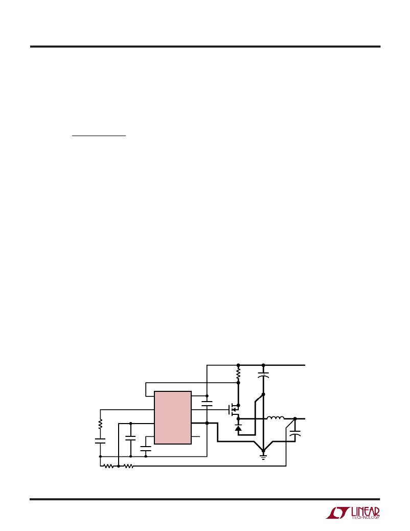
�PC� Board� Layout� Checklist�
�When� laying� out� the� printed� circuit� board,� the� following�
�checklist� should� be� used� to� ensure� proper� operation� of� the�
�LTC1622.� These� items� are� illustrated� graphically� in� the�
�layout� diagram� in� Figure� 6.� Check� the� following� in� your�
�layout:�
�1.� Is� the� Schottky� diode� closely� connected� between� ground�
�at� (–)� lead� of� C� IN� and� drain� of� the� external� MOSFET?�
�2.� Does� the� (+)� plate� of� C� IN� connect� to� the� sense� resistor�
�as� closely� as� possible?� This� capacitor� provides� AC�
�current� to� the� MOSFET.�
�3.� Is� the� input� decoupling� capacitor� (0.1� μ� F)� connected�
�closely� between� V� IN� (Pin� 8)� and� ground� (Pin� 6)?�
�4.� Connect� the� end� of� R� SENSE� as� close� to� V� IN� (Pin� 8)� as�
�possible.� The� V� IN� pin� is� the� SENSE� +� of� the� current�
�comparator.�
�5.� Is� the� trace� from� the� SENSE� –� (Pin� 1)� to� the� Sense�
�resistor� kept� short?� Does� the� trace� connect� close� to�
�R� SENSE� ?�
�6.� Keep� the� switching� node,� SW,� away� from� sensitive�
�small� signal� nodes.�
�7.� Does� the� V� FB� pin� connect� directly� to� the� feedback�
�resistors?� The� resistive� divider� R1� and� R2� must� be�
�connected� between� the� (+)� plate� of� C� OUT� and� signal�
�ground.� Optional� capacitor� C1� should� be� located� as�
�close� as� possible� to� the� LTC1622.�
�R1� and� R2� should� be� located� as� close� as� possible� to� the�
�LTC1622.� R2� should� connect� to� the� output� as� close� to�
�the� load� as� practicable.�
�R� SENSE�
�+�
�C� IN�
�V� IN�
�R� ITH�
�1�
�2�
�3�
�SENSE� –� V� IN�
�I� TH� PDRV�
�LTC1622�
�V� FB� GND�
�8�
�7�
�6�
�0.1� μ� F�
�M1�
�SW�
�L1�
�+�
�V� OUT�
�C� ITH�
�C1�
�4� RUN/�
�SS�
�SYNC/� 5�
�MODE�
�C� OUT�
�C� SS�
�QUIET� SGND�
�R1�
�R2�
�1622� F06�
�BOLD� LINES� INDICATE� HIGH� CURRENT� PATHS�
�Figure� 6.� LTC1622� Layout� Diagram� (See� PC� Board� Layout� Checklist)�
�12�
�相关PDF资料 |
PDF描述 |
|---|---|
| MIC2182-5.0YSM | IC REG CTRLR BUCK PWM CM 16-SSOP |
| SPD62-352M | INDUCTOR PWR SHIELDED 3.50UH SMD |
| SPD62-242M | INDUCTOR PWR SHIELDED 2.40UH SMD |
| URZ0J332MHD | CAP ALUM 3300UF 6.3V 20% RADIAL |
| UPM1A122MHD6 | CAP ALUM 1200UF 10V 20% RADIAL |
相关代理商/技术参数 |
参数描述 |
|---|---|
| LTC1623CMS8 | 功能描述:IC HI-SIDE SW CNTRLR DUAL 8-MSOP RoHS:否 类别:集成电路 (IC) >> PMIC - MOSFET,电桥驱动器 - 外部开关 系列:- 标准包装:5 系列:- 配置:低端 输入类型:非反相 延迟时间:600ns 电流 - 峰:12A 配置数:1 输出数:1 高端电压 - 最大(自引导启动):- 电源电压:14.2 V ~ 15.8 V 工作温度:-20°C ~ 60°C 安装类型:通孔 封装/外壳:21-SIP 模块 供应商设备封装:模块 包装:散装 配用:BG2A-NF-ND - KIT DEV BOARD FOR IGBT 其它名称:835-1063 |
| LTC1623CMS8#PBF | 功能描述:IC HI-SIDE SW CNTRLR DUAL 8-MSOP RoHS:是 类别:集成电路 (IC) >> PMIC - MOSFET,电桥驱动器 - 外部开关 系列:- 标准包装:50 系列:- 配置:高端 输入类型:非反相 延迟时间:200ns 电流 - 峰:250mA 配置数:1 输出数:1 高端电压 - 最大(自引导启动):600V 电源电压:12 V ~ 20 V 工作温度:-40°C ~ 125°C 安装类型:通孔 封装/外壳:8-DIP(0.300",7.62mm) 供应商设备封装:8-DIP 包装:管件 其它名称:*IR2127 |
| LTC1623CMS8#TR | 功能描述:IC CTRLR SW SMBUS DUAL 8MSOP RoHS:否 类别:集成电路 (IC) >> PMIC - MOSFET,电桥驱动器 - 外部开关 系列:- 标准包装:5 系列:- 配置:低端 输入类型:非反相 延迟时间:600ns 电流 - 峰:12A 配置数:1 输出数:1 高端电压 - 最大(自引导启动):- 电源电压:14.2 V ~ 15.8 V 工作温度:-20°C ~ 60°C 安装类型:通孔 封装/外壳:21-SIP 模块 供应商设备封装:模块 包装:散装 配用:BG2A-NF-ND - KIT DEV BOARD FOR IGBT 其它名称:835-1063 |
| LTC1623CMS8#TRPBF | 功能描述:IC HI-SIDE SW CNTRLR DUAL 8-MSOP RoHS:是 类别:集成电路 (IC) >> PMIC - MOSFET,电桥驱动器 - 外部开关 系列:- 标准包装:50 系列:- 配置:高端 输入类型:非反相 延迟时间:200ns 电流 - 峰:250mA 配置数:1 输出数:1 高端电压 - 最大(自引导启动):600V 电源电压:12 V ~ 20 V 工作温度:-40°C ~ 125°C 安装类型:通孔 封装/外壳:8-DIP(0.300",7.62mm) 供应商设备封装:8-DIP 包装:管件 其它名称:*IR2127 |
| LTC1623CS8 | 功能描述:IC HI-SIDE SW CNTRLR DUAL 8-SOIC RoHS:否 类别:集成电路 (IC) >> PMIC - MOSFET,电桥驱动器 - 外部开关 系列:- 标准包装:5 系列:- 配置:低端 输入类型:非反相 延迟时间:600ns 电流 - 峰:12A 配置数:1 输出数:1 高端电压 - 最大(自引导启动):- 电源电压:14.2 V ~ 15.8 V 工作温度:-20°C ~ 60°C 安装类型:通孔 封装/外壳:21-SIP 模块 供应商设备封装:模块 包装:散装 配用:BG2A-NF-ND - KIT DEV BOARD FOR IGBT 其它名称:835-1063 |
发布紧急采购,3分钟左右您将得到回复。