- 您现在的位置:买卖IC网 > PDF目录15503 > LTC1622IS8#PBF (Linear Technology)IC REG CTRLR BUCK PWM CM 8-SOIC PDF资料下载
参数资料
| 型号: | LTC1622IS8#PBF |
| 厂商: | Linear Technology |
| 文件页数: | 6/16页 |
| 文件大小: | 0K |
| 描述: | IC REG CTRLR BUCK PWM CM 8-SOIC |
| 标准包装: | 100 |
| PWM 型: | 电流模式 |
| 输出数: | 1 |
| 频率 - 最大: | 625kHz |
| 占空比: | 100% |
| 电源电压: | 2 V ~ 10 V |
| 降压: | 是 |
| 升压: | 无 |
| 回扫: | 无 |
| 反相: | 无 |
| 倍增器: | 无 |
| 除法器: | 无 |
| Cuk: | 无 |
| 隔离: | 无 |
| 工作温度: | -45°C ~ 85°C |
| 封装/外壳: | 8-SOIC(0.154",3.90mm 宽) |
| 包装: | 管件 |
�� �
�
�LTC1622�
�OPERATIO�
�(Refer� to� Functional� Diagram)�
�the� I� TH� pin� will� drop.� When� the� I� TH� voltage� goes� below�
�0.12V,� the� sleep� signal� goes� high,� turning� off� the� external�
�MOSFET.� The� sleep� signal� goes� low� when� the� I� TH� voltage�
�rises� above� 0.22V� and� the� LTC1622� resumes� normal�
�operation.� The� next� oscillator� cycle� will� turn� the� external�
�MOSFET� on� and� the� switching� cycle� repeats.�
�Frequency� Synchronization�
�The� LTC1622� can� be� externally� driven� by� a� TTL/CMOS�
�compatible� clock� signal� up� to� 750kHz.� Do� not� synchronize�
�the� LTC1622� below� its� maximum� default� operating� fre-�
�quency� of� 625kHz� as� this� may� cause� abnormal� operation�
�and� an� undesired� frequency� spectrum.� The� LTC1622� is�
�synchronized� to� the� rising� edge� of� the� clock.� The� external�
�clock� pulse� width� must� be� at� least� 100ns� and� not� more�
�than� the� period� minus� 200ns.�
�Synchronization� is� inhibited� when� the� feedback� voltage� is�
�below� 0.3V.� This� is� to� prevent� inductor� current� buildup�
�under� short-circuit� conditions.� Burst� Mode� operation� is�
�deactivated� when� the� LTC1622� is� externally� driven� by� a�
�Short-Circuit� Protection�
�When� the� output� is� shorted� to� ground,� the� frequency� of� the�
�oscillator� will� be� reduced� to� about� 110kHz.� This� lower�
�frequency� allows� the� inductor� current� to� safely� discharge,�
�thereby� preventing� current� runaway.� The� oscillator’s� fre-�
�quency� will� gradually� increase� to� its� nominal� value� when�
�the� feedback� voltage� increases� above� 0.65V.� Note� that�
�synchronization� is� inhibited� until� the� feedback� voltage�
�goes� above� 0.3V.�
�Overvoltage� Protection�
�As� a� further� protection,� the� overvoltage� comparator� in� the�
�LTC1622� will� turn� the� external� MOSFET� off� when� the�
�feedback� voltage� has� risen� 16%� above� the� reference�
�voltage� of� 0.8V.� This� comparator� has� a� typical� hysteresis�
�of� 35mV.�
�Slope� Compensation� and� Peak� Inductor� Current�
�The� inductor’s� peak� current� is� determined� by:�
�(�
�clock.�
�Dropout� Operation�
�I� PK� =�
�V� ITH�
�10� R� SENSE�
�)�
�When� the� input� supply� voltage� decreases� towards� the�
�output� voltage,� the� rate� of� change� of� inductor� current�
�during� the� ON� cycle� decreases.� This� reduction� means� that�
�the� P-channel� MOSFET� will� remain� on� for� more� than� one�
�oscillator� cycle� since� the� inductor� current� has� not� ramped�
�up� to� the� threshold� set� by� EA.� Further� reduction� in� input�
�supply� voltage� will� eventually� cause� the� P-channel� MOSFET�
�to� be� turned� on� 100%,� i.e.,� DC.� The� output� voltage� will� then�
�be� determined� by� the� input� voltage� minus� the� voltage� drop�
�across� the� MOSFET,� the� sense� resistor� and� the� inductor.�
�Undervoltage� Lockout�
�when� the� LTC1622� is� operating� below� 40%� duty� cycle.�
�However,� once� the� duty� cycle� exceeds� 40%,� slope� com-�
�pensation� begins� and� effectively� reduces� the� peak� induc-�
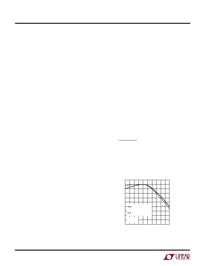
�tor� current.� The� amount� of� reduction� is� given� by� the� curves�
�in� Figure� 2.�
�110�
�100�
�90�
�80�
�70�
�60�
�To� prevent� operation� of� the� P-channel� MOSFET� below� safe�
�input� voltage� levels,� an� undervoltage� lockout� is� incorpo-�
�rated� into� the� LTC1622.� When� the� input� supply� voltage�
�drops� below� 2V,� the� P-channel� MOSFET� and� all� circuitry� is�
�turned� off� except� the� undervoltage� block,� which� draws�
�only� several� microamperes.�
�50�
�40�
�30�
�20�
�10�
�0�
�I� RIPPLE� =� 0.4I� PK�
�AT� 5%� DUTY� CYCLE�
�I� RIPPLE� =� 0.2I� PK�
�AT� 5%� DUTY� CYCLE�
�V� IN� =� 4.2V�
�UNSYNC�
�10� 20� 30� 40� 50� 60� 70� 80� 90� 100�
�DUTY� CYCLE� (%)�
�1622� F02�
�Figure� 2.� Maximum� Output� Current� vs� Duty� Cycle�
�6�
�相关PDF资料 |
PDF描述 |
|---|---|
| MIC2182-5.0YSM | IC REG CTRLR BUCK PWM CM 16-SSOP |
| SPD62-352M | INDUCTOR PWR SHIELDED 3.50UH SMD |
| SPD62-242M | INDUCTOR PWR SHIELDED 2.40UH SMD |
| URZ0J332MHD | CAP ALUM 3300UF 6.3V 20% RADIAL |
| UPM1A122MHD6 | CAP ALUM 1200UF 10V 20% RADIAL |
相关代理商/技术参数 |
参数描述 |
|---|---|
| LTC1623CMS8 | 功能描述:IC HI-SIDE SW CNTRLR DUAL 8-MSOP RoHS:否 类别:集成电路 (IC) >> PMIC - MOSFET,电桥驱动器 - 外部开关 系列:- 标准包装:5 系列:- 配置:低端 输入类型:非反相 延迟时间:600ns 电流 - 峰:12A 配置数:1 输出数:1 高端电压 - 最大(自引导启动):- 电源电压:14.2 V ~ 15.8 V 工作温度:-20°C ~ 60°C 安装类型:通孔 封装/外壳:21-SIP 模块 供应商设备封装:模块 包装:散装 配用:BG2A-NF-ND - KIT DEV BOARD FOR IGBT 其它名称:835-1063 |
| LTC1623CMS8#PBF | 功能描述:IC HI-SIDE SW CNTRLR DUAL 8-MSOP RoHS:是 类别:集成电路 (IC) >> PMIC - MOSFET,电桥驱动器 - 外部开关 系列:- 标准包装:50 系列:- 配置:高端 输入类型:非反相 延迟时间:200ns 电流 - 峰:250mA 配置数:1 输出数:1 高端电压 - 最大(自引导启动):600V 电源电压:12 V ~ 20 V 工作温度:-40°C ~ 125°C 安装类型:通孔 封装/外壳:8-DIP(0.300",7.62mm) 供应商设备封装:8-DIP 包装:管件 其它名称:*IR2127 |
| LTC1623CMS8#TR | 功能描述:IC CTRLR SW SMBUS DUAL 8MSOP RoHS:否 类别:集成电路 (IC) >> PMIC - MOSFET,电桥驱动器 - 外部开关 系列:- 标准包装:5 系列:- 配置:低端 输入类型:非反相 延迟时间:600ns 电流 - 峰:12A 配置数:1 输出数:1 高端电压 - 最大(自引导启动):- 电源电压:14.2 V ~ 15.8 V 工作温度:-20°C ~ 60°C 安装类型:通孔 封装/外壳:21-SIP 模块 供应商设备封装:模块 包装:散装 配用:BG2A-NF-ND - KIT DEV BOARD FOR IGBT 其它名称:835-1063 |
| LTC1623CMS8#TRPBF | 功能描述:IC HI-SIDE SW CNTRLR DUAL 8-MSOP RoHS:是 类别:集成电路 (IC) >> PMIC - MOSFET,电桥驱动器 - 外部开关 系列:- 标准包装:50 系列:- 配置:高端 输入类型:非反相 延迟时间:200ns 电流 - 峰:250mA 配置数:1 输出数:1 高端电压 - 最大(自引导启动):600V 电源电压:12 V ~ 20 V 工作温度:-40°C ~ 125°C 安装类型:通孔 封装/外壳:8-DIP(0.300",7.62mm) 供应商设备封装:8-DIP 包装:管件 其它名称:*IR2127 |
| LTC1623CS8 | 功能描述:IC HI-SIDE SW CNTRLR DUAL 8-SOIC RoHS:否 类别:集成电路 (IC) >> PMIC - MOSFET,电桥驱动器 - 外部开关 系列:- 标准包装:5 系列:- 配置:低端 输入类型:非反相 延迟时间:600ns 电流 - 峰:12A 配置数:1 输出数:1 高端电压 - 最大(自引导启动):- 电源电压:14.2 V ~ 15.8 V 工作温度:-20°C ~ 60°C 安装类型:通孔 封装/外壳:21-SIP 模块 供应商设备封装:模块 包装:散装 配用:BG2A-NF-ND - KIT DEV BOARD FOR IGBT 其它名称:835-1063 |
发布紧急采购,3分钟左右您将得到回复。