- 您现在的位置:买卖IC网 > PDF目录14136 > LTC1627CS8#TR (Linear Technology)IC REG BUCK SYNC ADJ 0.5A 8SOIC PDF资料下载
参数资料
| 型号: | LTC1627CS8#TR |
| 厂商: | Linear Technology |
| 文件页数: | 7/16页 |
| 文件大小: | 0K |
| 描述: | IC REG BUCK SYNC ADJ 0.5A 8SOIC |
| 标准包装: | 2,500 |
| 类型: | 降压(降压) |
| 输出类型: | 可调式 |
| 输出数: | 1 |
| 输出电压: | 0.8 V ~ 8.5 V |
| 输入电压: | 2.65 V ~ 8.5 V |
| PWM 型: | 电流模式,混合 |
| 频率 - 开关: | 35kHz ~ 350kHz |
| 电流 - 输出: | 500mA |
| 同步整流器: | 是 |
| 工作温度: | 0°C ~ 70°C |
| 安装类型: | 表面贴装 |
| 封装/外壳: | 8-SOIC(0.154",3.90mm 宽) |
| 包装: | 带卷 (TR) |
| 供应商设备封装: | 8-SOIC |
�� �
�
�LTC1627�
�OPERATIO�
�load� slightly� allows� constant� frequency� PWM� operation�
�to� resume.�
�Frequency� synchronization� is� inhibited� when� the� feedback�
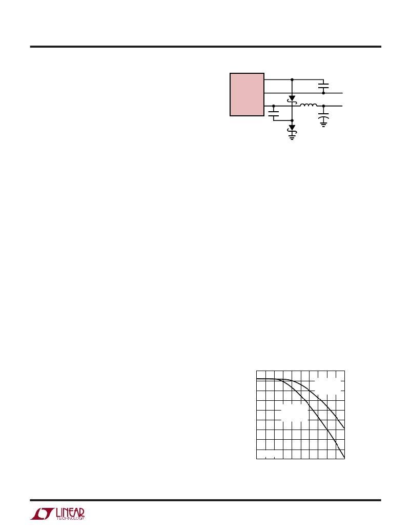
�V� DR�
�LTC1627� V� IN�
�D1� L1�
�C1�
�0.1� μ� F�
�V� IN� <� 4.5V�
�voltage� V� FB� is� below� 0.6V.� This� prevents� the� external� clock�
�from� interfering� with� the� frequency� foldback� for� short-�
�SW�
�C2�
�0.1� μ� F�
�+�
�C� OUT�
�100� μ� F�
�V� OUT�
�circuit� protection.�
�D2�
�1627� F02�
�Dropout� Operation�
�When� the� input� supply� voltage� decreases� toward� the� out-�
�put� voltage,� the� duty� cycle� increases� toward� the� maximum�
�on-time.� Further� reduction� of� the� supply� voltage� forces� the�
�main� switch� to� remain� on� for� more� than� one� cycle� until� it�
�reaches� 100%� duty� cycle.� The� output� voltage� will� then� be�
�determined� by� the� input� voltage� minus� the� voltage� drop�
�across� the� P-channel� MOSFET� and� the� inductor.�
�In� Burst� Mode� operation� or� pulse� skipping� mode� operation�
�(externally� synchronized)� with� the� output� lightly� loaded,�
�the� LTC1627� transitions� through� continuous� mode� as� it�
�enters� dropout.�
�Undervoltage� Lockout�
�A� precision� undervoltage� lockout� shuts� down� the� LTC1627�
�when� V� IN� drops� below� 2.5V,� making� it� ideal� for� single�
�lithium-ion� battery� applications.� In� lockout,� the� LTC1627�
�draws� only� several� microamperes,� which� is� low� enough� to�
�prevent� deep� discharge� and� possible� damage� to� the� lithium-�
�ion� battery� nearing� its� end� of� charge.� A� 150mV� hysteresis�
�ensures� reliable� operation� with� noisy� supplies.�
�Low� Supply� Operation�
�The� LTC1627� is� designed� to� operate� down� to� 2.65V� supply�
�Figure� 2.� Using� a� Charge� Pump� to� Bias� V� DR�
�the� charge� pump� at� V� IN� ≥� 4.5V� is� not� recommended� to�
�ensure� that� (V� IN� –� V� DR� )� does� not� exceed� its� absolute�
�maximum� voltage.�
�When� V� IN� decreases� to� a� voltage� close� to� V� OUT� ,� the� loop�
�may� enter� dropout� and� attempt� to� turn� on� the� P-channel�
�MOSFET� continuously.� When� the� V� DR� charge� pump� is�
�enabled,� a� dropout� detector� counts� the� number� of� oscilla-�
�tor� cycles� that� the� P-channel� MOSFET� remains� on,� and�
�periodically� forces� a� brief� off� period� to� allow� C1� to�
�recharge.� 100%� duty� cycle� is� allowed� when� V� DR� is� grounded.�
�Slope� Compensation� and� Inductor� Peak� Current�
�Slope� compensation� provides� stability� by� preventing�
�subharmonic� oscillations.� It� works� by� internally� adding� a�
�ramp� to� the� inductor� current� signal� at� duty� cycles� in� excess�
�of� 40%.� As� a� result,� the� maximum� inductor� peak� current�
�is� lower� for� V� OUT� /V� IN� >� 0.4� than� when� V� OUT� /V� IN� <� 0.4.� See�
�the� inductor� peak� current� as� a� function� of� duty� cycle� graph�
�in� Figure� 3.� The� worst-case� peak� current� reduction� occurs�
�with� the� oscillator� synchronized� at� its� minimum� frequency,�
�i.e.,� to� a� clock� just� above� the� oscillator� free-running�
�950�
�voltage.� At� this� voltage� the� converter� is� most� likely� to� be�
�900�
�WITHOUT�
�running� at� high� duty� cycles� or� in� dropout� where� the� main�
�switch� is� on� continuously.� Hence,� the� I� 2� R� loss� is� due�
�mainly� to� the� R� DS(ON)� of� the� P-channel� MOSFET.� See�
�Efficiency� Considerations� in� the� Applications� Information�
�section.�
�When� V� IN� is� low� (<� 4.5V)� the� R� DS(ON)� of� the� P-channel�
�MOSFET� can� be� lowered� by� driving� its� gate� below� ground.�
�The� top� P-channel� MOSFET� driver� makes� use� of� a� floating�
�850�
�800�
�750�
�700�
�650�
�600�
�550�
�500�
�V� IN� = 5V�
�WORST� CASE�
�EXTERNAL�
�CLOCK� SYNC�
�EXTERNAL�
�CLOCK� SYNC�
�return� pin,� V� DR� ,� to� allow� biasing� below� GND.� A� simple�
�charge� pump� bootstrapped� to� the� SW� pin� realizes� a�
�negative� voltage� at� the� V� DR� pin� as� shown� in� Figure� 2.� Using�
�0� 10� 20� 30� 40� 50� 60� 70� 80� 90� 100�
�DUTY� CYCLE� (%)�
�1627� F03�
�Figure� 3.� Maximum� Inductor� Peak� Current� vs� Duty� Cycle�
�7�
�相关PDF资料 |
PDF描述 |
|---|---|
| LTC1503IS8-2#TRPBF | IC REG BUCK SWITCHD CAP 2V 8SOIC |
| LTC1503IS8-2#TR | IC REG BUCK SWITCHD CAP 2V 8SOIC |
| LTC1503IS8-1.8#TR | IC REG BUCK SWITCHED CAP 8SOIC |
| HSM18DRXI | CONN EDGECARD 36POS DIP .156 SLD |
| HMM18DRXI | CONN EDGECARD 36POS DIP .156 SLD |
相关代理商/技术参数 |
参数描述 |
|---|---|
| LTC1627IS8 | 功能描述:IC REG BUCK SYNC ADJ 0.5A 8SOIC RoHS:否 类别:集成电路 (IC) >> PMIC - 稳压器 - DC DC 开关稳压器 系列:- 标准包装:2,500 系列:- 类型:降压(降压) 输出类型:固定 输出数:1 输出电压:1.2V,1.5V,1.8V,2.5V 输入电压:2.7 V ~ 20 V PWM 型:- 频率 - 开关:- 电流 - 输出:50mA 同步整流器:是 工作温度:-40°C ~ 125°C 安装类型:表面贴装 封装/外壳:10-TFSOP,10-MSOP(0.118",3.00mm 宽)裸露焊盘 包装:带卷 (TR) 供应商设备封装:10-MSOP 裸露焊盘 |
| LTC1627IS8#PBF | 功能描述:IC REG BUCK SYNC ADJ 0.5A 8SOIC RoHS:是 类别:集成电路 (IC) >> PMIC - 稳压器 - DC DC 开关稳压器 系列:- 标准包装:250 系列:- 类型:降压(降压) 输出类型:固定 输出数:1 输出电压:1.2V 输入电压:2.05 V ~ 6 V PWM 型:电压模式 频率 - 开关:2MHz 电流 - 输出:500mA 同步整流器:是 工作温度:-40°C ~ 85°C 安装类型:表面贴装 封装/外壳:6-UFDFN 包装:带卷 (TR) 供应商设备封装:6-SON(1.45x1) 产品目录页面:1032 (CN2011-ZH PDF) 其它名称:296-25628-2 |
| LTC1627IS8#TR | 功能描述:IC REG BUCK SYNC ADJ 0.5A 8SOIC RoHS:否 类别:集成电路 (IC) >> PMIC - 稳压器 - DC DC 开关稳压器 系列:- 标准包装:2,500 系列:- 类型:降压(降压) 输出类型:固定 输出数:1 输出电压:1.2V,1.5V,1.8V,2.5V 输入电压:2.7 V ~ 20 V PWM 型:- 频率 - 开关:- 电流 - 输出:50mA 同步整流器:是 工作温度:-40°C ~ 125°C 安装类型:表面贴装 封装/外壳:10-TFSOP,10-MSOP(0.118",3.00mm 宽)裸露焊盘 包装:带卷 (TR) 供应商设备封装:10-MSOP 裸露焊盘 |
| LTC1627IS8#TRPBF | 功能描述:IC REG BUCK SYNC ADJ 0.5A 8SOIC RoHS:是 类别:集成电路 (IC) >> PMIC - 稳压器 - DC DC 开关稳压器 系列:- 标准包装:2,500 系列:- 类型:降压(降压) 输出类型:固定 输出数:1 输出电压:1.2V,1.5V,1.8V,2.5V 输入电压:2.7 V ~ 20 V PWM 型:- 频率 - 开关:- 电流 - 输出:50mA 同步整流器:是 工作温度:-40°C ~ 125°C 安装类型:表面贴装 封装/外壳:10-TFSOP,10-MSOP(0.118",3.00mm 宽)裸露焊盘 包装:带卷 (TR) 供应商设备封装:10-MSOP 裸露焊盘 |
| LTC1628CG | 功能描述:IC REG CTRLR BUCK PWM CM 28-SSOP RoHS:否 类别:集成电路 (IC) >> PMIC - 稳压器 - DC DC 切换控制器 系列:- 标准包装:4,500 系列:PowerWise® PWM 型:控制器 输出数:1 频率 - 最大:1MHz 占空比:95% 电源电压:2.8 V ~ 5.5 V 降压:是 升压:无 回扫:无 反相:无 倍增器:无 除法器:无 Cuk:无 隔离:无 工作温度:-40°C ~ 125°C 封装/外壳:6-WDFN 裸露焊盘 包装:带卷 (TR) 配用:LM1771EVAL-ND - BOARD EVALUATION LM1771 其它名称:LM1771SSDX |
发布紧急采购,3分钟左右您将得到回复。