- 您现在的位置:买卖IC网 > PDF目录15237 > LTC1629IG-PG (Linear Technology)IC REG CTRLR BUCK PWM CM 28-SSOP PDF资料下载
参数资料
| 型号: | LTC1629IG-PG |
| 厂商: | Linear Technology |
| 文件页数: | 14/28页 |
| 文件大小: | 0K |
| 描述: | IC REG CTRLR BUCK PWM CM 28-SSOP |
| 标准包装: | 47 |
| 系列: | PolyPhase® |
| PWM 型: | 电流模式 |
| 输出数: | 1 |
| 频率 - 最大: | 360kHz |
| 占空比: | 99.5% |
| 电源电压: | 4 V ~ 36 V |
| 降压: | 是 |
| 升压: | 无 |
| 回扫: | 无 |
| 反相: | 无 |
| 倍增器: | 无 |
| 除法器: | 无 |
| Cuk: | 无 |
| 隔离: | 无 |
| 工作温度: | -40°C ~ 85°C |
| 封装/外壳: | 28-SSOP(0.209",5.30mm 宽) |
| 包装: | 管件 |
第1页第2页第3页第4页第5页第6页第7页第8页第9页第10页第11页第12页第13页当前第14页第15页第16页第17页第18页第19页第20页第21页第22页第23页第24页第25页第26页第27页第28页
�� �
�
�LTC1629/LTC1629-PG�
�APPLICATIO� S� I� FOR� ATIO�
�?� I�
�?�
�V�
�P� MAIN� =� OUT� ?� MAX� ?� (� 1� +� δ� )� R� DS� (� ON� )� +�
�k� (� V� IN� )� ?� MAX� ?� (� C� RSS� )(� )�
�2� ?� I� ?�
�?� N� ?�
�?� I�
�?�
�(� )�
�P� SYNC� =� IN� OUT� ?� MAX� ?� 1� +� δ� R� DS� (� ON� )�
�The MOSFET power dissipations at maximum output�
�current� are� given� by:�
�2�
�V� IN� ?� N� ?�
�f�
�2�
�V� –� V�
�V� IN� ?� N� ?�
�where� δ� is� the� temperature� dependency� of� R� DS(ON)� ,� k� is� a�
�constant� inversely� related� to� the� gate� drive� current� and� N�
�is� the� number� of� stages.�
�Both� MOSFETs� have� I� 2� R� losses� but� the� topside� N-channel�
�additional� transition� losses� due� to� their� larger� junction�
�capacitance.�
�C� IN� and� C� OUT� Selection�
�In� continuous� mode,� the� source� current� of� each� top�
�N-channel� MOSFET� is� a� square� wave� of� duty� cycle� V� OUT� /�
�V� IN� .� A� low� ESR� input� capacitor� sized� for� the� maximum�
�RMS� current� must� be� used.� The� details� of� a� close� form�
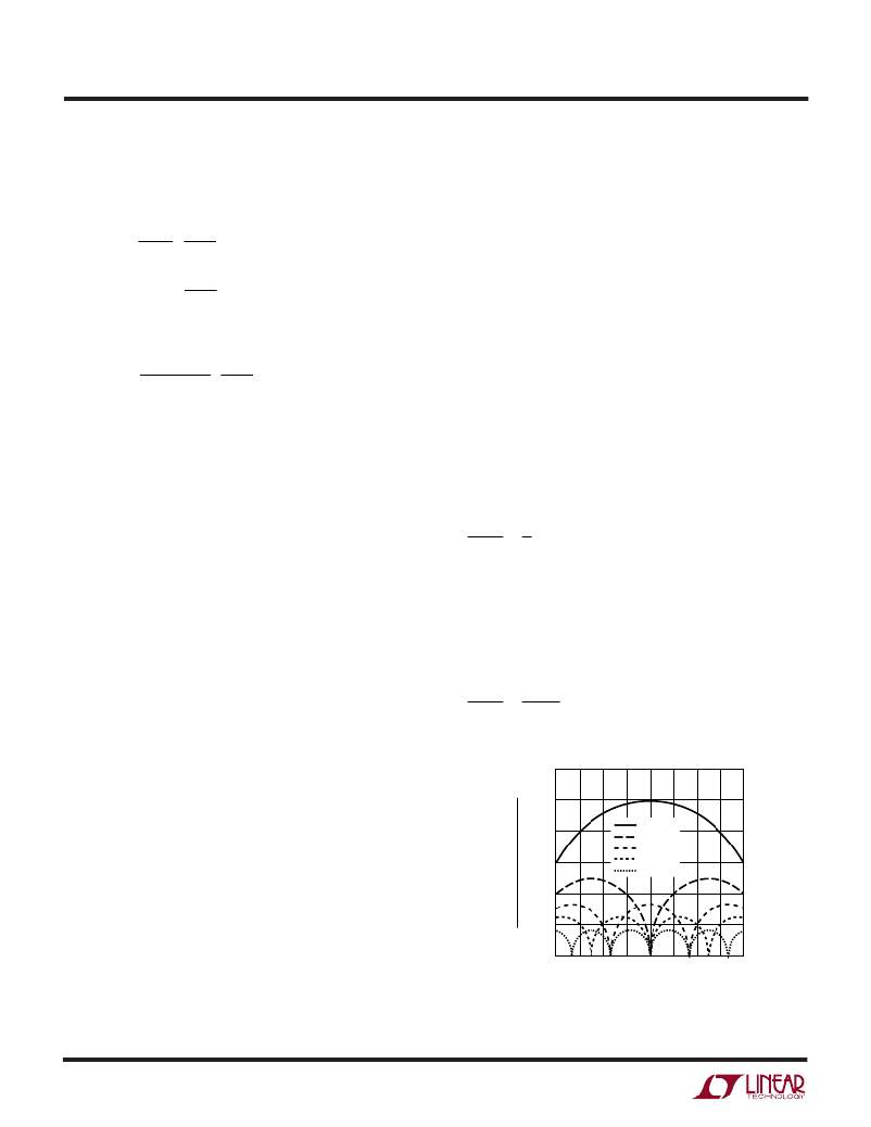
�equation� can� be� found� in� Application� Note� 77.� Figure� 4�
�shows� the� input� capacitor� ripple� current� for� different�
�phase� configurations� with� the� output� voltage� fixed� and�
�input� voltage� varied.� The� input� ripple� current� is� normalized�
�against� the� DC� output� current.� The� graph� can� be� used� in�
�place� of� tedious� calculations.� The� minimum� input� ripple�
�current� can� be� achieved� when� the� product� of� phase� num-�
�ber� and� output� voltage,� N(V� OUT� ),� is� approximately� equal� to�
�the� input� voltage� V� IN� or:�
�equation� includes� an� additional� term� for� transition� losses,�
�which� peak� at� the� highest� input� voltage.� For� V� IN� <� 20V� the�
�high� current� efficiency� generally� improves� with� larger�
�V� OUT�
�V� IN�
�=�
�k�
�N�
�where� k� =� 1,� 2,� …,� N� –� 1�
�MOSFETs,� while� for� V� IN� >� 20V� the� transition� losses� rapidly�
�increase� to� the� point� that� the� use� of� a� higher� R� DS(ON)� device�
�with� lower� C� RSS� actual� provides� higher� efficiency.� The�
�synchronous� MOSFET� losses� are� greatest� at� high� input�
�voltage� when� the� top� switch� duty� factor� is� low� or� during� a�
�So� the� phase� number� can� be� chosen� to� minimize� the� input�
�capacitor� size� for� the� given� input� and� output� voltages.�
�In� the� graph� of� Figure� 4,� the� local� maximum� input� RMS�
�capacitor� currents� are� reached� when:�
�short-circuit� when� the� synchronous� switch� is� on� close� to�
�100%� of� the� period.�
�The� term� (1� +� δ� )� is� generally� given� for� a� MOSFET� in� the�
�V� OUT�
�V� IN�
�=�
�2� k� ?� 1�
�2� N�
�where� k� =� 1,� 2,� …,� N�
�form� of� a� normalized� R� DS(ON)� vs.� Temperature� curve,� but�
�δ� =� 0.005/� °� C� can� be� used� as� an� approximation� for� low�
�voltage� MOSFETs.� C� RSS� is� usually� specified� in� the� MOS-�
�FET� characteristics.� The� constant� k� =� 1.7� can� be� used� to�
�0.6�
�0.5�
�estimate� the� contributions� of� the� two� terms� in� the� main�
�switch� dissipation� equation.�
�The� Schottky� diodes,� D1� and� D2� shown� in� Figure� 1� conduct�
�during� the� dead-time� between� the� conduction� of� the� two�
�large� power� MOSFETs.� This� helps� prevent� the� body� diode�
�of� the� bottom� MOSFET� from� turning� on,� storing� charge�
�0.4�
�0.3�
�0.2�
�0.1�
�1-PHASE�
�2-PHASE�
�3-PHASE�
�4-PHASE�
�6-PHASE�
�during� the� dead-time,� and� requiring� a� reverse� recovery�
�period� which� would� reduce� efficiency.� A� 1A� to� 3A� (depend-�
�ing� on� output� current)� Schottky� diode� is� generally� a� good�
�0�
�0.1�
�0.2�
�0.3� 0.4� 0.5� 0.6� 0.7�
�DUTY� FACTOR� (V� OUT� /V� IN� )�
�0.8� 0.9�
�1629� F04�
�compromise� for� both� regions� of� operation� due� to� the�
�relatively� small� average� current.� Larger� diodes� result� in�
�14�
�Figure� 4.� Normalized� Input� RMS� Ripple� Current� vs�
�Duty� Factor� for� 1� to� 6� Output� Stages�
�相关PDF资料 |
PDF描述 |
|---|---|
| LTC3703IGN-5#PBF | IC REG CTRLR BST PWM VM 16-SSOP |
| LT3757MPMSE#TRPBF | IC REG CTRLR PWM CM 10-MSOP |
| NCP304HSQ30T1G | IC VOLT DETECT CMOS 3.0V SC-82AB |
| ISC1210EB150J | INDUCTOR WW 15UH 5% 1210 |
| LTC3890HUH#TRPBF | IC REG CTRLR BUCK PWM CM 32-QFN |
相关代理商/技术参数 |
参数描述 |
|---|---|
| LTC1629IG-PG#PBF | 功能描述:IC REG CTRLR BUCK PWM CM 28-SSOP RoHS:是 类别:集成电路 (IC) >> PMIC - 稳压器 - DC DC 切换控制器 系列:PolyPhase® 标准包装:4,500 系列:PowerWise® PWM 型:控制器 输出数:1 频率 - 最大:1MHz 占空比:95% 电源电压:2.8 V ~ 5.5 V 降压:是 升压:无 回扫:无 反相:无 倍增器:无 除法器:无 Cuk:无 隔离:无 工作温度:-40°C ~ 125°C 封装/外壳:6-WDFN 裸露焊盘 包装:带卷 (TR) 配用:LM1771EVAL-ND - BOARD EVALUATION LM1771 其它名称:LM1771SSDX |
| LTC1629IG-PG#TR | 功能描述:IC REG CTRLR BUCK PWM CM 28-SSOP RoHS:否 类别:集成电路 (IC) >> PMIC - 稳压器 - DC DC 切换控制器 系列:PolyPhase® 标准包装:4,500 系列:PowerWise® PWM 型:控制器 输出数:1 频率 - 最大:1MHz 占空比:95% 电源电压:2.8 V ~ 5.5 V 降压:是 升压:无 回扫:无 反相:无 倍增器:无 除法器:无 Cuk:无 隔离:无 工作温度:-40°C ~ 125°C 封装/外壳:6-WDFN 裸露焊盘 包装:带卷 (TR) 配用:LM1771EVAL-ND - BOARD EVALUATION LM1771 其它名称:LM1771SSDX |
| LTC1629IG-PG#TRPBF | 功能描述:IC REG CTRLR BUCK PWM CM 28-SSOP RoHS:是 类别:集成电路 (IC) >> PMIC - 稳压器 - DC DC 切换控制器 系列:PolyPhase® 标准包装:4,500 系列:PowerWise® PWM 型:控制器 输出数:1 频率 - 最大:1MHz 占空比:95% 电源电压:2.8 V ~ 5.5 V 降压:是 升压:无 回扫:无 反相:无 倍增器:无 除法器:无 Cuk:无 隔离:无 工作温度:-40°C ~ 125°C 封装/外壳:6-WDFN 裸露焊盘 包装:带卷 (TR) 配用:LM1771EVAL-ND - BOARD EVALUATION LM1771 其它名称:LM1771SSDX |
| LTC1642ACGN | 制造商:Linear Technology 功能描述:Hot Swap Controller 1-CH 16.5V 16-Pin SSOP N |
| LTC1642ACGN#PBF | 功能描述:IC CONTROLLER HOTSWAP ADJ 16SSOP RoHS:是 类别:集成电路 (IC) >> PMIC - 热交换 系列:- 产品培训模块:Obsolescence Mitigation Program 标准包装:100 系列:- 类型:热插拔开关 应用:通用 内部开关:是 电流限制:可调 电源电压:9 V ~ 13.2 V 工作温度:-40°C ~ 150°C 安装类型:表面贴装 封装/外壳:10-WFDFN 裸露焊盘 供应商设备封装:10-TDFN-EP(3x3) 包装:管件 |
发布紧急采购,3分钟左右您将得到回复。