- 您现在的位置:买卖IC网 > PDF目录2004 > LTC1667CG#PBF (Linear Technology)IC D/A CONV 14BIT 50MSPS 28-SSOP PDF资料下载
参数资料
| 型号: | LTC1667CG#PBF |
| 厂商: | Linear Technology |
| 文件页数: | 7/24页 |
| 文件大小: | 0K |
| 描述: | IC D/A CONV 14BIT 50MSPS 28-SSOP |
| 标准包装: | 47 |
| 设置时间: | 20ns |
| 位数: | 14 |
| 数据接口: | 并联 |
| 转换器数目: | 1 |
| 电压电源: | 双 ± |
| 功率耗散(最大): | 180mW |
| 工作温度: | 0°C ~ 70°C |
| 安装类型: | 表面贴装 |
| 封装/外壳: | 28-SSOP(0.209",5.30mm 宽) |
| 供应商设备封装: | 28-SSOP |
| 包装: | 管件 |
| 输出数目和类型: | 2 电流,单极 |
| 采样率(每秒): | 50M |
| 产品目录页面: | 1352 (CN2011-ZH PDF) |
15
LTC1666/LTC1667/LTC1668
APPLICATIO S I FOR ATIO
WU
UU
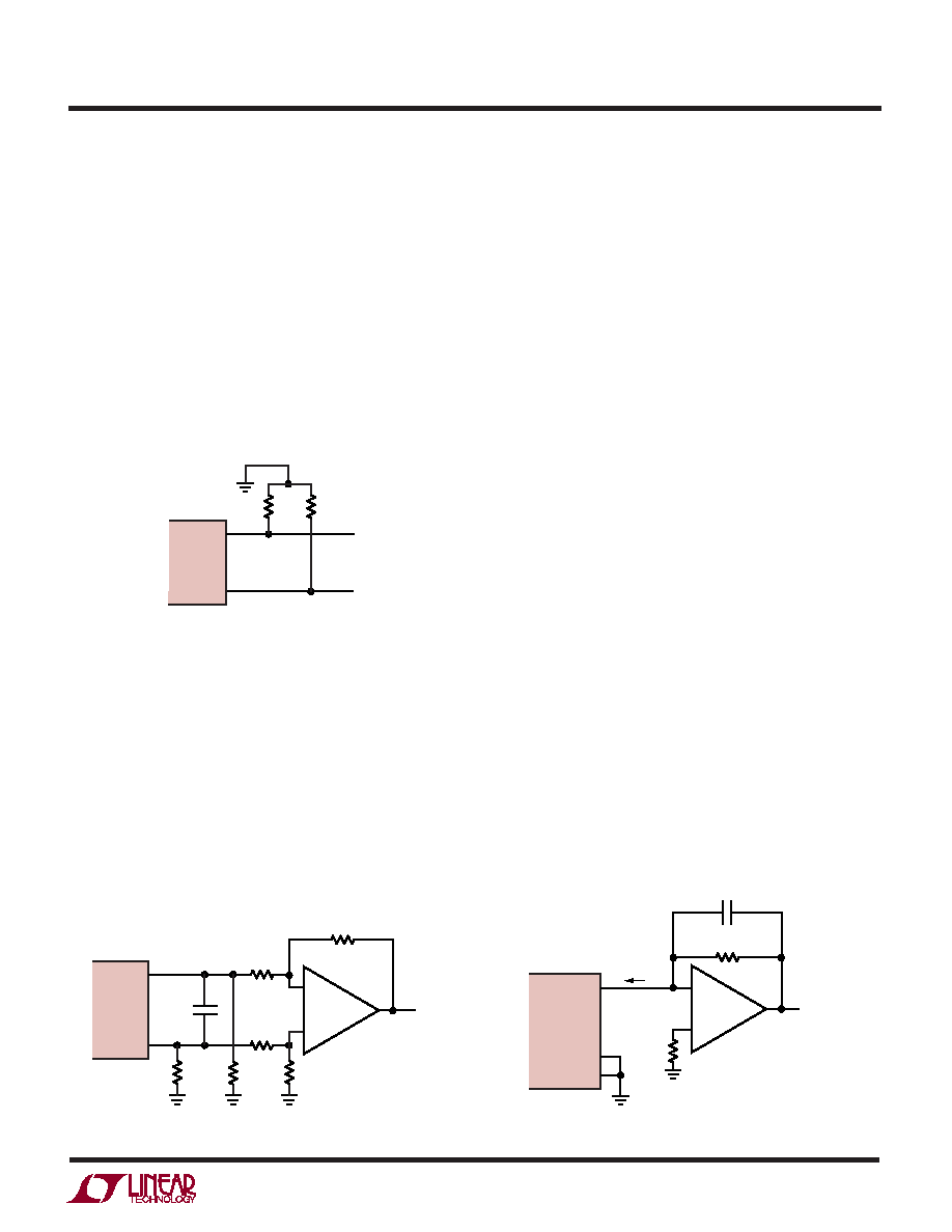
Resistor Loaded Outputs
A differential resistor loaded output configuration is shown
in Figure 6. It is simple and economical, but it can drive
only differential loads with impedance levels and ampli-
tudes appropriate for the DAC outputs.
The recommended single-ended resistor loaded configu-
ration is essentially the same circuit as the differential
resistor loaded, case—simply use the IOUT A output,
referred to ground. Rather than tying the unused IOUT B
output to ground, it is preferred to load it with the equiva-
lent RLOAD of IOUT A. Then IOUT B will still swing with a
waveform complementary to IOUT A.
helps reduce distortion by limiting the high frequency
signal amplitude at the op amp inputs. The circuit swings
±1V around ground.
Figure 8 shows a simplified circuit for a single-ended
output using I-to-V converter to produce a unipolar
buffered voltage output. This configuration typically has
the best DC linearity performance, but its AC distortion at
higher frequencies is limited by U1’s slewing capabilities.
Digital Interface
The LTC1666/LTC1667/LTC1668 have parallel inputs that
are latched on the rising edge of the clock input. They
accept CMOS levels from either 5V or 3.3V logic and can
accept clock rates of up to 50MHz.
Referring to the Timing Diagram and Block Diagram, the
data inputs go to master-slave latches that update on the
rising edge of the clock. The input logic thresholds, VIH =
2.4V min, VIL = 0.8V max, work with 3.3V or 5V CMOS
levels over temperature. The guaranteed setup time, tDS,
is 8ns minimum and the hold time, tDH, is 4ns minimum.
The minimum clock high and low times are guaranteed at
6ns and 8ns, respectively. These specifications allow the
LTC1666/LTC1667/LTC1668 to be clocked at up to 50Msps
minimum.
For best AC performance, the data and clock waveforms
need to be clean and free of undershoot and overshoot.
Clock and data interconnect lines should be twisted pair,
coax or microstrip, and proper line termination is impor-
tant. If the digital input signals to the DAC are considered
as analog AC voltage signals, they are rich in spectral
components over a broad frequency range, usually in-
Op Amp I to V Converter Outputs
Adding an op amp differential to single-ended converter
circuit to the differential resistor loaded output gives the
circuit of Figure 7.
This circuit complements the capabilities of the trans-
former-coupled application at lower frequencies, since
available op amps can deliver good AC distortion perfor-
mance at signal frequencies of a few MHz down to DC. The
optional capacitor adds a single real pole of filtering, and
Figure 6. Differential Resistor-Loaded Output
IOUT B
IOUT A
52.3
52.3
1666/7/8 F07
LTC1666/
LTC1667/
LTC1668
Figure 8. Single-Ended Op Amp I to V Converter
200
1666/7/8 F09
IOUT A
IOUT B
LADCOM
RFB
200
VOUT
0V TO 2V
IOUTFS
10mA
COUT
–
+
U1
LT
1812
LTC1666/
LTC1667/
LTC1668
IOUT B
IOUT A
52.3
500
52.3
1666/7/8 F08
–
+
200
500
200
60pF
LT1809
±1V
10dBm
VOUT
LTC1666/
LTC1667/
LTC1668
Figure 7. Differential to Single-Ended Op Amp I-V Converter
相关PDF资料 |
PDF描述 |
|---|---|
| LTC1686IS8#TRPBF | IC TXRX RS485 PREC DELAY 8-SOIC |
| LTC1688IS | IC DVR 100MBPS RS485 QUAD 16SOIC |
| LTC1690IS8#TRPBF | IC RCVR/DVR PAIR LOW PWR 8-SOIC |
| LTC1740IG#TRPBF | IC ADC 14BIT 6MSPS 36SSOP |
| LTC1741IFW#PBF | IC ADC 12BIT 65MSPS 48-TSSOP |
相关代理商/技术参数 |
参数描述 |
|---|---|
| LTC1667IG | 功能描述:IC D/A CONV 14BIT 50MSPS 28-SSOP RoHS:否 类别:集成电路 (IC) >> 数据采集 - 数模转换器 系列:- 产品培训模块:Data Converter Fundamentals DAC Architectures 标准包装:750 系列:- 设置时间:7µs 位数:16 数据接口:并联 转换器数目:1 电压电源:双 ± 功率耗散(最大):100mW 工作温度:0°C ~ 70°C 安装类型:表面贴装 封装/外壳:28-LCC(J 形引线) 供应商设备封装:28-PLCC(11.51x11.51) 包装:带卷 (TR) 输出数目和类型:1 电压,单极;1 电压,双极 采样率(每秒):143k |
| LTC1667IG#PBF | 功能描述:IC D/A CONV 14BIT 50MSPS 28-SSOP RoHS:是 类别:集成电路 (IC) >> 数据采集 - 数模转换器 系列:- 产品培训模块:Data Converter Fundamentals DAC Architectures 标准包装:750 系列:- 设置时间:7µs 位数:16 数据接口:并联 转换器数目:1 电压电源:双 ± 功率耗散(最大):100mW 工作温度:0°C ~ 70°C 安装类型:表面贴装 封装/外壳:28-LCC(J 形引线) 供应商设备封装:28-PLCC(11.51x11.51) 包装:带卷 (TR) 输出数目和类型:1 电压,单极;1 电压,双极 采样率(每秒):143k |
| LTC1667IG#TR | 功能描述:IC D/A CONV 14BIT 50MSPS 28-SSOP RoHS:否 类别:集成电路 (IC) >> 数据采集 - 数模转换器 系列:- 产品培训模块:Data Converter Fundamentals DAC Architectures 标准包装:750 系列:- 设置时间:7µs 位数:16 数据接口:并联 转换器数目:1 电压电源:双 ± 功率耗散(最大):100mW 工作温度:0°C ~ 70°C 安装类型:表面贴装 封装/外壳:28-LCC(J 形引线) 供应商设备封装:28-PLCC(11.51x11.51) 包装:带卷 (TR) 输出数目和类型:1 电压,单极;1 电压,双极 采样率(每秒):143k |
| LTC1667IG#TRPBF | 功能描述:IC D/A CONV 14BIT 50MSPS 28-SSOP RoHS:是 类别:集成电路 (IC) >> 数据采集 - 数模转换器 系列:- 产品培训模块:Data Converter Fundamentals DAC Architectures 标准包装:750 系列:- 设置时间:7µs 位数:16 数据接口:并联 转换器数目:1 电压电源:双 ± 功率耗散(最大):100mW 工作温度:0°C ~ 70°C 安装类型:表面贴装 封装/外壳:28-LCC(J 形引线) 供应商设备封装:28-PLCC(11.51x11.51) 包装:带卷 (TR) 输出数目和类型:1 电压,单极;1 电压,双极 采样率(每秒):143k |
| LTC1668CG | 功能描述:IC D/A CONV 16BIT 50MSPS 28-SSOP RoHS:否 类别:集成电路 (IC) >> 数据采集 - 数模转换器 系列:- 产品培训模块:Data Converter Fundamentals DAC Architectures 标准包装:750 系列:- 设置时间:7µs 位数:16 数据接口:并联 转换器数目:1 电压电源:双 ± 功率耗散(最大):100mW 工作温度:0°C ~ 70°C 安装类型:表面贴装 封装/外壳:28-LCC(J 形引线) 供应商设备封装:28-PLCC(11.51x11.51) 包装:带卷 (TR) 输出数目和类型:1 电压,单极;1 电压,双极 采样率(每秒):143k |
发布紧急采购,3分钟左右您将得到回复。