- 您现在的位置:买卖IC网 > PDF目录2004 > LTC1667CG#PBF (Linear Technology)IC D/A CONV 14BIT 50MSPS 28-SSOP PDF资料下载
参数资料
| 型号: | LTC1667CG#PBF |
| 厂商: | Linear Technology |
| 文件页数: | 8/24页 |
| 文件大小: | 0K |
| 描述: | IC D/A CONV 14BIT 50MSPS 28-SSOP |
| 标准包装: | 47 |
| 设置时间: | 20ns |
| 位数: | 14 |
| 数据接口: | 并联 |
| 转换器数目: | 1 |
| 电压电源: | 双 ± |
| 功率耗散(最大): | 180mW |
| 工作温度: | 0°C ~ 70°C |
| 安装类型: | 表面贴装 |
| 封装/外壳: | 28-SSOP(0.209",5.30mm 宽) |
| 供应商设备封装: | 28-SSOP |
| 包装: | 管件 |
| 输出数目和类型: | 2 电流,单极 |
| 采样率(每秒): | 50M |
| 产品目录页面: | 1352 (CN2011-ZH PDF) |
16
LTC1666/LTC1667/LTC1668
APPLICATIO S I FOR ATIO
WU
UU
cluding the output signal band of interest. Therefore, any
direct coupling of the digital signals to the analog output
will produce spurious tones that vary with the exact digital
input pattern.
Clock jitter should be minimized to avoid degrading the
noise floor of the device in AC applications, especially
where high output frequencies are being generated. Any
noise coupling from the digital inputs to the clock input will
cause phase modulation of the clock signal and the DAC
waveform, and can produce spurious tones. It is normally
best to place the digital data transitions near the falling
clock edge, well away from the active rising clock edge.
Because the clock signal contains spectral components
only at the sampling frequency and its multiples, it is
usually not a source of in band spurious tones. Overall, it
is better to treat the clock as you would an analog signal
and route it separately from the digital data input signals.
The clock trace should be routed either over the analog
ground plane or over its own section of the ground plane.
The clock line needs to have accurately controlled imped-
ance and should be well terminated near the LTC1666/
LTC1667/LTC1668.
Printed Circuit Board Layout Considerations—
Grounding, Bypassing and Output Signal Routing
The close proximity of high frequency digital data lines and
high dynamic range, wide-band analog signals makes
clean printed circuit board design and layout an absolute
necessity. Figures 11 to 15 are the printed circuit board
layers for an AC evaluation circuit for the LTC1668. Ground
planes should be split between digital and analog sections
as shown. All bypass capacitors should have minimum
trace length and be ceramic 0.1
F or larger with low ESR.
Bypass capacitors are required on VSS, VDD and REFOUT,
and all connected to the AGND plane. The COMP2 pin ties
to a node in the output current switching circuitry, and it
requires a 0.1
F bypass capacitor. It should be bypassed
to VSS along with COMP1. The AGND and DGND pins
should both tie directly to the AGND plane, and the tie point
between the AGND and DGND planes should nominally be
near the DGND pin. LADCOM should either be tied directly
to the AGND plane or be bypassed to AGND. The IOUTA and
IOUT B traces should be close together, short, and well
matched for good AC CMRR. The transformer output
ground should be capable of optionally being isolated or
being tied to the AGND plane, depending on which gives
better performance in the system.
Suggested Evaluation Circuit
Figure 10 is the schematic and Figures 11 to 15 are the
circuit board layouts for a suggested evaluation circuit,
DC245A. The circuit can be programmed with component
selection and jumpers for a variety of differentially coupled
transformer output and differential and single-ended re-
sistor loaded output configurations.
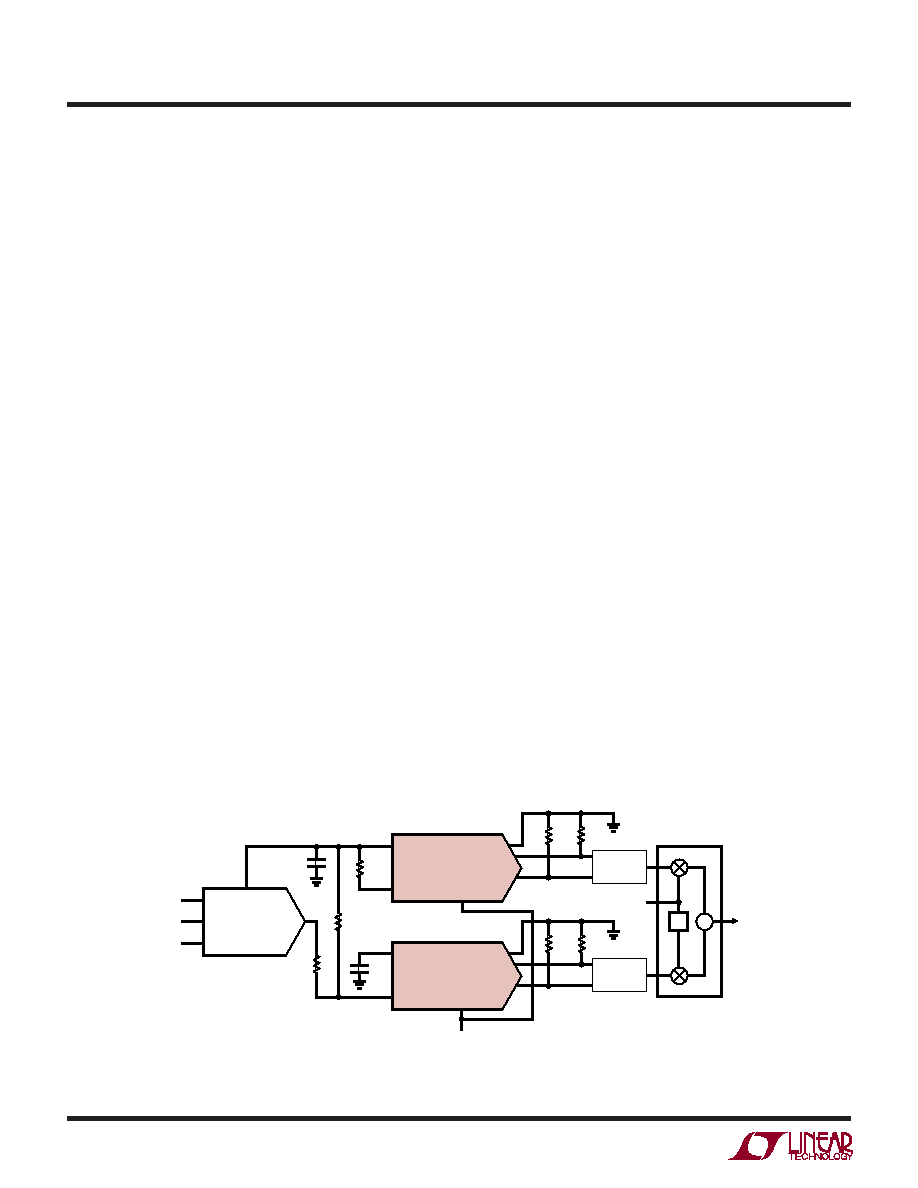
REFOUT
LADCOM
IOUT A
VOUT
IOUT B
I
REFIN
CLK
LTC1668
U2
Q-CHANNEL
REFOUT
LADCOM
IOUT A
IOUT B
I
REFIN
CLK
LTC1668
U1
I-CHANNEL
52.3
52.3
52.3
52.3
LOW-PASS
FILTER
LOW-PASS
FILTER
CLOCK
INPUT
REF
1/2 LTC1661
U3
SERIAL
INPUT
2k
2.1k
21k
0.1
F
0.1
F
90
°
∑
LOCAL
OSCILLATOR
QAM
OUTPUT
QUADRATURE
MODULATOR
±5%
RELATIVE GAIN
ADJUSTMENT RANGE
1666/7/8 F10
Figure 9. QAM Modulation Using LTC1668 with
Digitally Controlled I vs Q Channel Gain Adjustment
相关PDF资料 |
PDF描述 |
|---|---|
| LTC1686IS8#TRPBF | IC TXRX RS485 PREC DELAY 8-SOIC |
| LTC1688IS | IC DVR 100MBPS RS485 QUAD 16SOIC |
| LTC1690IS8#TRPBF | IC RCVR/DVR PAIR LOW PWR 8-SOIC |
| LTC1740IG#TRPBF | IC ADC 14BIT 6MSPS 36SSOP |
| LTC1741IFW#PBF | IC ADC 12BIT 65MSPS 48-TSSOP |
相关代理商/技术参数 |
参数描述 |
|---|---|
| LTC1667IG | 功能描述:IC D/A CONV 14BIT 50MSPS 28-SSOP RoHS:否 类别:集成电路 (IC) >> 数据采集 - 数模转换器 系列:- 产品培训模块:Data Converter Fundamentals DAC Architectures 标准包装:750 系列:- 设置时间:7µs 位数:16 数据接口:并联 转换器数目:1 电压电源:双 ± 功率耗散(最大):100mW 工作温度:0°C ~ 70°C 安装类型:表面贴装 封装/外壳:28-LCC(J 形引线) 供应商设备封装:28-PLCC(11.51x11.51) 包装:带卷 (TR) 输出数目和类型:1 电压,单极;1 电压,双极 采样率(每秒):143k |
| LTC1667IG#PBF | 功能描述:IC D/A CONV 14BIT 50MSPS 28-SSOP RoHS:是 类别:集成电路 (IC) >> 数据采集 - 数模转换器 系列:- 产品培训模块:Data Converter Fundamentals DAC Architectures 标准包装:750 系列:- 设置时间:7µs 位数:16 数据接口:并联 转换器数目:1 电压电源:双 ± 功率耗散(最大):100mW 工作温度:0°C ~ 70°C 安装类型:表面贴装 封装/外壳:28-LCC(J 形引线) 供应商设备封装:28-PLCC(11.51x11.51) 包装:带卷 (TR) 输出数目和类型:1 电压,单极;1 电压,双极 采样率(每秒):143k |
| LTC1667IG#TR | 功能描述:IC D/A CONV 14BIT 50MSPS 28-SSOP RoHS:否 类别:集成电路 (IC) >> 数据采集 - 数模转换器 系列:- 产品培训模块:Data Converter Fundamentals DAC Architectures 标准包装:750 系列:- 设置时间:7µs 位数:16 数据接口:并联 转换器数目:1 电压电源:双 ± 功率耗散(最大):100mW 工作温度:0°C ~ 70°C 安装类型:表面贴装 封装/外壳:28-LCC(J 形引线) 供应商设备封装:28-PLCC(11.51x11.51) 包装:带卷 (TR) 输出数目和类型:1 电压,单极;1 电压,双极 采样率(每秒):143k |
| LTC1667IG#TRPBF | 功能描述:IC D/A CONV 14BIT 50MSPS 28-SSOP RoHS:是 类别:集成电路 (IC) >> 数据采集 - 数模转换器 系列:- 产品培训模块:Data Converter Fundamentals DAC Architectures 标准包装:750 系列:- 设置时间:7µs 位数:16 数据接口:并联 转换器数目:1 电压电源:双 ± 功率耗散(最大):100mW 工作温度:0°C ~ 70°C 安装类型:表面贴装 封装/外壳:28-LCC(J 形引线) 供应商设备封装:28-PLCC(11.51x11.51) 包装:带卷 (TR) 输出数目和类型:1 电压,单极;1 电压,双极 采样率(每秒):143k |
| LTC1668CG | 功能描述:IC D/A CONV 16BIT 50MSPS 28-SSOP RoHS:否 类别:集成电路 (IC) >> 数据采集 - 数模转换器 系列:- 产品培训模块:Data Converter Fundamentals DAC Architectures 标准包装:750 系列:- 设置时间:7µs 位数:16 数据接口:并联 转换器数目:1 电压电源:双 ± 功率耗散(最大):100mW 工作温度:0°C ~ 70°C 安装类型:表面贴装 封装/外壳:28-LCC(J 形引线) 供应商设备封装:28-PLCC(11.51x11.51) 包装:带卷 (TR) 输出数目和类型:1 电压,单极;1 电压,双极 采样率(每秒):143k |
发布紧急采购,3分钟左右您将得到回复。