- 您现在的位置:买卖IC网 > PDF目录15265 > LTC1702IGN#TRPBF (Linear Technology)IC REG CTRLR BUCK PWM VM 24-SSOP PDF资料下载
参数资料
| 型号: | LTC1702IGN#TRPBF |
| 厂商: | Linear Technology |
| 文件页数: | 10/36页 |
| 文件大小: | 0K |
| 描述: | IC REG CTRLR BUCK PWM VM 24-SSOP |
| 标准包装: | 2,500 |
| 系列: | PolyPhase® |
| PWM 型: | 电压模式 |
| 输出数: | 2 |
| 频率 - 最大: | 750kHz |
| 占空比: | 93% |
| 电源电压: | 3 V ~ 7 V |
| 降压: | 是 |
| 升压: | 无 |
| 回扫: | 无 |
| 反相: | 无 |
| 倍增器: | 无 |
| 除法器: | 无 |
| Cuk: | 无 |
| 隔离: | 无 |
| 工作温度: | -40°C ~ 85°C |
| 封装/外壳: | 24-SSOP(0.154",3.90mm 宽) |
| 包装: | 带卷 (TR) |
第1页第2页第3页第4页第5页第6页第7页第8页第9页当前第10页第11页第12页第13页第14页第15页第16页第17页第18页第19页第20页第21页第22页第23页第24页第25页第26页第27页第28页第29页第30页第31页第32页第33页第34页第35页第36页
�� �
�
�LTC1702�
�APPLICATIO� N� S� I� N� FOR� M� ATIO� N�
�amp� of� continuous� current� with� peak� currents� up� to� 5A� to�
�slew� large� MOSFET� gates� quickly.� The� external� MOSFETs�
�are� connected� with� the� drain� of� QT� attached� to� the� input�
�supply� and� the� source� of� QT� at� the� switching� node� SW.� QB�
�is� the� synchronous� rectifier� with� its� drain� at� SW� and� its�
�source� at� PGND.� SW� is� connected� to� one� end� of� the�
�inductor,� with� the� other� end� connected� to� V� OUT� .� The� output�
�capacitor is connected from V� OUT� to PGND.�
�When� a� switching� cycle� begins,� QB� is� turned� off� and� QT� is�
�turned� on.� SW� rises� almost� immediately� to� V� IN� and� the�
�inductor� current� begins� to� increase.� When� the� PWM� pulse�
�finishes,� QT� turns� off� and� one� nonoverlap� interval� later,� QB�
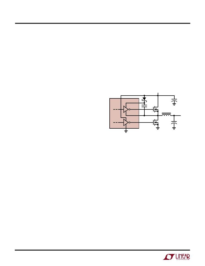
�tion� with� a� simple� external� charge� pump� (Figure� 2),� this�
�allows� the� LTC1702� to� completely� enhance� the� gate� of� QT�
�without� requiring� an� additional,� higher� supply� voltage.�
�The� two� channels� of� the� LTC1702� run� from� a� common�
�clock,� with� the� phasing� chosen� to� be� 180� °� from� side� 1� to�
�side� 2.� This� has� the� effect� of� doubling� the� frequency� of� the�
�switching� pulses� seen� by� the� input� bypass� capacitor,� sig-�
�nificantly� lowering� the� RMS� current� seen� by� the� capacitor�
�and� reducing� the� value� required� (see� the� 2-Phase� section).�
�V� IN�
�turns� on.� Now� SW� drops� to� PGND� and� the� inductor� current�
�decreases.� The� cycle� repeats� with� the� next� tick� of� the�
�PV� CC�
�BOOST�
�D� CP�
�+�
�C� IN�
�master� clock.� The� percentage� of� time� spent� in� each� mode�
�is� controlled� by� the� duty� cycle� of� the� PWM� signal,� which� in�
�turn� is� controlled� by� the� feedback� amplifier.� The� master�
�TG�
�SW�
�C� CP�
�1� μ� F�
�QT�
�L� EXT�
�V� OUT�
�clock� generates� a� 1V� P-P� ,� 550kHz� sawtooth� waveform� and�
�turns� QT� once� every� 1.8� μ� s.� In� a� typical� application� with� a�
�5V� input� and� a� 1.6V� output,� the� duty� cycle� will� be� set� at� 1.6/�
�5� � 100%� or� 32%� by� the� feedback� loop.� This� will� give�
�roughly� a� 575ns� on-time� for� QT� and� a� 1.22� μ� s� on-time� for�
�QB.�
�LTC1702�
�BG�
�QB�
�PGND�
�Figure� 2.� Floating� TG� Driver� Supply�
�+�
�C� OUT�
�1702� F02�
�This� constant� frequency� operation� brings� with� it� a� couple�
�of� benefits.� Inductor� and� capacitor� values� can� be� chosen�
�with� a� precise� operating� frequency� in� mind� and� the� feed-�
�back� loop� components� can� be� similarly� tightly� specified.�
�Noise� generated� by� the� circuit� will� always� be� in� a� known�
�frequency� band� with� the� 550kHz� frequency� designed� to�
�leave� the� 455kHz� IF� band� free� of� interference.� Subharmonic�
�oscillation� and� slope� compensation,� common� headaches�
�with� constant� frequency� current� mode� switchers,� are�
�absent� in� voltage� mode� designs� like� the� LTC1702.�
�During� the� time� that� QT� is� on,� its� source� (the� SW� pin)� is� at�
�V� IN� .� V� IN� is� also� the� power� supply� for� the� LTC1702.� How-�
�ever,� QT� requires� V� IN� +� V� GS(ON)� at� its� gate� to� achieve�
�minimum� R� ON� .� This� presents� a� problem� for� the� LTC1702—�
�it� needs� to� generate� a� gate� drive� signal� at� TG� higher� than�
�its� highest� supply� voltage.� To� get� around� this,� the� TG� driver�
�runs� from� floating� supplies,� with� its� negative� supply� at-�
�tached� to� SW� and� its� power� supply� at� BOOST.� This� allows�
�it� to� slew� up� and� down� with� the� source� of� QT.� In� combina-�
�Feedback� Amplifier�
�Each� side� of� the� LTC1702� senses� the� output� voltage� at�
�V� OUT� with� an� internal� feedback� op� amp� (see� Block� Dia-�
�gram).� This� is� a� real� op� amp� with� a� low� impedance� output,�
�85dB� open-loop� gain� and� 25MHz� gain-bandwidth� product.�
�The� positive� input� is� connected� internally� to� an� 800mV�
�reference,� while� the� negative� input� is� connected� to� the� FB�
�pin.� The� output� is� connected� to� COMP,� which� is� in� turn�
�connected� to� the� soft-start� circuitry� and� from� there� to� the�
�PWM� generator.�
�Unlike� many� regulators� that� use� a� resistor� divider� con-�
�nected� to� a� high� impedance� feedback� input,� the� LTC1702�
�is� designed� to� use� an� inverting� summing� amplifier� topol-�
�ogy� with� the� FB� pin� configured� as� a� virtual� ground.� This�
�allows� flexibility� in� choosing� pole� and� zero� locations� not�
�available� with� simple� g� m� configurations.� In� particular,� it�
�allows� the� use� of� “type� 3”� compensation,� which� provides�
�a� phase� boost� at� the� LC� pole� frequency� and� significantly�
�1702fa�
�10�
�相关PDF资料 |
PDF描述 |
|---|---|
| H2AXT-10112-Y4-ND | JUMPER-H1502TR/A2015Y/X 12" |
| LTC1873EG#TRPBF | IC REG CTRLR BUCK PWM VM 28-SSOP |
| H2AXT-10112-W4-ND | JUMPER-H1502TR/A2015W/X 12" |
| LTC1159CG-5 | IC REG CTRLR BUCK PWM CM 20-SSOP |
| LTC1159CG-3.3#PBF | IC REG CTRLR BUCK PWM CM 20-SSOP |
相关代理商/技术参数 |
参数描述 |
|---|---|
| LTC1703CG | 功能描述:IC REG SW DUAL SYNC VID 28SSOP RoHS:否 类别:集成电路 (IC) >> PMIC - 稳压器 - 专用型 系列:- 标准包装:43 系列:- 应用:控制器,Intel VR11 输入电压:5 V ~ 12 V 输出数:1 输出电压:0.5 V ~ 1.6 V 工作温度:-40°C ~ 85°C 安装类型:表面贴装 封装/外壳:48-VFQFN 裸露焊盘 供应商设备封装:48-QFN(7x7) 包装:管件 |
| LTC1703CG#PBF | 功能描述:IC REG SW DUAL SYNC VID 28SSOP RoHS:是 类别:集成电路 (IC) >> PMIC - 稳压器 - 专用型 系列:- 标准包装:2,000 系列:- 应用:控制器,DSP 输入电压:4.5 V ~ 25 V 输出数:2 输出电压:最低可调至 1.2V 工作温度:-40°C ~ 85°C 安装类型:表面贴装 封装/外壳:30-TFSOP(0.173",4.40mm 宽) 供应商设备封装:30-TSSOP 包装:带卷 (TR) |
| LTC1703CG#TR | 制造商:Linear Technology 功能描述:LDO Cntrlr REG CTRLR 0.9V to 2V 28-Pin SSOP T/R |
| LTC1703CG#TRPBF | 功能描述:IC REG SW DUAL SYNC VID 28SSOP RoHS:是 类别:集成电路 (IC) >> PMIC - 稳压器 - 专用型 系列:- 标准包装:43 系列:- 应用:控制器,Intel VR11 输入电压:5 V ~ 12 V 输出数:1 输出电压:0.5 V ~ 1.6 V 工作温度:-40°C ~ 85°C 安装类型:表面贴装 封装/外壳:48-VFQFN 裸露焊盘 供应商设备封装:48-QFN(7x7) 包装:管件 |
| LTC1703IG | 功能描述:IC REG SW DL SYNC W/VID 28-SSOP RoHS:否 类别:集成电路 (IC) >> PMIC - 稳压器 - 专用型 系列:- 标准包装:43 系列:- 应用:控制器,Intel VR11 输入电压:5 V ~ 12 V 输出数:1 输出电压:0.5 V ~ 1.6 V 工作温度:-40°C ~ 85°C 安装类型:表面贴装 封装/外壳:48-VFQFN 裸露焊盘 供应商设备封装:48-QFN(7x7) 包装:管件 |
发布紧急采购,3分钟左右您将得到回复。