- 您现在的位置:买卖IC网 > PDF目录15265 > LTC1702IGN#TRPBF (Linear Technology)IC REG CTRLR BUCK PWM VM 24-SSOP PDF资料下载
参数资料
| 型号: | LTC1702IGN#TRPBF |
| 厂商: | Linear Technology |
| 文件页数: | 11/36页 |
| 文件大小: | 0K |
| 描述: | IC REG CTRLR BUCK PWM VM 24-SSOP |
| 标准包装: | 2,500 |
| 系列: | PolyPhase® |
| PWM 型: | 电压模式 |
| 输出数: | 2 |
| 频率 - 最大: | 750kHz |
| 占空比: | 93% |
| 电源电压: | 3 V ~ 7 V |
| 降压: | 是 |
| 升压: | 无 |
| 回扫: | 无 |
| 反相: | 无 |
| 倍增器: | 无 |
| 除法器: | 无 |
| Cuk: | 无 |
| 隔离: | 无 |
| 工作温度: | -40°C ~ 85°C |
| 封装/外壳: | 24-SSOP(0.154",3.90mm 宽) |
| 包装: | 带卷 (TR) |
第1页第2页第3页第4页第5页第6页第7页第8页第9页第10页当前第11页第12页第13页第14页第15页第16页第17页第18页第19页第20页第21页第22页第23页第24页第25页第26页第27页第28页第29页第30页第31页第32页第33页第34页第35页第36页
�� �
�
�LTC1702�
�APPLICATIO� N� S� I� N� FOR� M� ATIO� N�
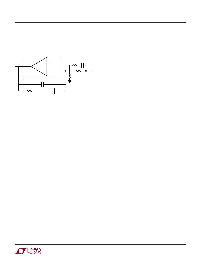
�improves� loop� phase� margin� (see� Figure� 3).� The� Feedback�
�Loop/Compensation� section� contains� a� detailed� explana-�
�tion� of� type� 3� feedback� loops.�
�Notice� that� the� FB� pin� is� the� virtual� ground� node� of� the�
�feedback� amplifier.� A� typical� compensation� network� does�
�not� include� local� DC� feedback� around� the� amplifier,� so� that�
�the� DC� level� at� FB� will� be� an� accurate� replica� of� the� output�
�voltage,� divided� down� by� R1� and� R� B� (Figure� 3).� However,�
�COMP�
�FB�
�C2�
�+�
�–�
�0.8V�
�FB�
�R3�
�R� B�
�R1�
�C3�
�V� OUT�
�the� compensation� capacitors� will� tend� to� attenuate� AC�
�signals� at� FB,� especially� with� low� bandwidth� type� 1� feed-�
�back� loops.� This� creates� a� situation� where� the� MIN� and�
�MAX� comparators� do� not� respond� immediately� to� shifts� in�
�the� output� voltage,� since� they� monitor� the� output� at� FB.�
�Maximizing� feedback� loop� bandwidth� will� minimize� these�
�R2�
�C1�
�delays� and� allow� MIN� and� MAX� to� operate� properly.� See�
�1702� F03�
�Figure� 3.� “Type� 3”� Feedback� Loop�
�MIN/MAX�
�Two� additional� feedback� loops� keep� an� eye� on� the� primary�
�feedback� amplifier� and� step� in� if� the� feedback� node� moves�
�±� 5%� from� its� nominal� 800mV� value.� The� MAX� comparator�
�(see� Block� Diagram)� activates� whenever� FB� rises� more�
�than� 5%� above� 800mV.� It� immediately� turns� the� top�
�MOSFET� (QT)� off� and� the� bottom� MOSFET� (QB)� on� and�
�keeps� them� that� way� until� FB� falls� back� within� 5%.� This�
�pulls� the� output� down� as� fast� as� possible,� preventing�
�damage� to� the� (often� expensive)� load.� If� FB� rises� because�
�the� output� is� shorted� to� a� higher� supply,� QB� will� stay� on�
�until� the� short� goes� away,� the� higher� supply� current� limits�
�or� QB� dies� trying� to� save� the� load.� This� behavior� provides�
�maximum� protection� against� overvoltage� faults� at� the�
�output,� while� allowing� the� circuit� to� resume� normal� opera-�
�tion� when� the� fault� is� removed.� The� overvoltage� protection�
�circuit� can� optionally� be� set� to� latch� the� output� off� perma-�
�nently� (see� the� Overvoltage� Fault� section).�
�The� MIN� comparator� (see� Block� Diagram)� trips� whenever�
�FB� is� more� than� 5%� below� 800mV� and� immediately� forces�
�the� switch� duty� cycle� to� 90%� to� bring� the� output� voltage�
�back� into� range.� It� releases� when� FB� is� within� the� 5%�
�window.� MIN� is� disabled� when� the� soft-start� or� current�
�limit� circuits� are� active� —the� only� two� times� that� the�
�output� should� legitimately� be� below� its� regulated� value.�
�the� Feedback� Loop/Compensation� section.�
�PGOOD� Flags�
�The� MIN� comparator� performs� another� function;� it� drives�
�the� external� “power� good”� pin� (PGOOD)� through� a� 100� μ� s�
�delay� stage.� PGOOD� is� an� open-drain� output,� allowing� it� to�
�be� wire-OR’ed� with� other� open-drain/open-collector� sig-�
�nals.� An� external� pull-up� resistor� is� required� for� PGOOD� to�
�swing� high.� Any� time� the� FB� pin� is� more� than� 5%� below� the�
�programmed� value� for� more� than� 100� μ� s,� PGOOD� will� pull�
�low,� indicating� that� the� output� is� out� of� regulation.� PGOOD�
�remains� active� during� soft-start� and� current� limit,� even�
�though� the� MIN� comparator� has� no� effect� on� the� duty� cycle�
�during� these� times.� The� 100� μ� s� delay� ensures� that� short�
�output� transient� glitches� that� are� successfully� “caught”� by�
�the� MIN� comparator� don’t� cause� momentary� glitches� at�
�the� PGOOD� pin.� Note� that� the� PGOOD� pin� only� watches�
�MIN,� not� MAX—it� does� not� indicate� if� the� output� is� 5%�
�above� the� programmed� value.�
�When� either� side� of� the� LTC1702� is� in� shutdown,� its�
�associated� PGOOD� pin� will� go� high.� This� behavior� allows�
�a� valid� PGOOD� reading� when� the� two� PGOOD� pins� are� tied�
�together,� even� if� one� side� is� shut� down.� It� also� reduces�
�quiescent� current� by� eliminating� the� excess� current� drawn�
�by� the� pull-up� at� the� PGOOD� pin.� As� soon� as� the� RUN/SS�
�pin� rises� above� the� shutdown� threshold� and� the� side�
�comes� out� of� shutdown,� the� PGOOD� pin� will� pull� low� until�
�the� output� voltage� is� valid.� If� both� sides� are� shut� down� at�
�the� same� time,� both� PGOOD� pins� will� go� high.� To� avoid�
�confusion,� if� either� side� of� the� LTC1702� is� shut� down,� the�
�host� system� should� ignore� the� associated� PGOOD� pin.�
�1702fa�
�11�
�相关PDF资料 |
PDF描述 |
|---|---|
| H2AXT-10112-Y4-ND | JUMPER-H1502TR/A2015Y/X 12" |
| LTC1873EG#TRPBF | IC REG CTRLR BUCK PWM VM 28-SSOP |
| H2AXT-10112-W4-ND | JUMPER-H1502TR/A2015W/X 12" |
| LTC1159CG-5 | IC REG CTRLR BUCK PWM CM 20-SSOP |
| LTC1159CG-3.3#PBF | IC REG CTRLR BUCK PWM CM 20-SSOP |
相关代理商/技术参数 |
参数描述 |
|---|---|
| LTC1703CG | 功能描述:IC REG SW DUAL SYNC VID 28SSOP RoHS:否 类别:集成电路 (IC) >> PMIC - 稳压器 - 专用型 系列:- 标准包装:43 系列:- 应用:控制器,Intel VR11 输入电压:5 V ~ 12 V 输出数:1 输出电压:0.5 V ~ 1.6 V 工作温度:-40°C ~ 85°C 安装类型:表面贴装 封装/外壳:48-VFQFN 裸露焊盘 供应商设备封装:48-QFN(7x7) 包装:管件 |
| LTC1703CG#PBF | 功能描述:IC REG SW DUAL SYNC VID 28SSOP RoHS:是 类别:集成电路 (IC) >> PMIC - 稳压器 - 专用型 系列:- 标准包装:2,000 系列:- 应用:控制器,DSP 输入电压:4.5 V ~ 25 V 输出数:2 输出电压:最低可调至 1.2V 工作温度:-40°C ~ 85°C 安装类型:表面贴装 封装/外壳:30-TFSOP(0.173",4.40mm 宽) 供应商设备封装:30-TSSOP 包装:带卷 (TR) |
| LTC1703CG#TR | 制造商:Linear Technology 功能描述:LDO Cntrlr REG CTRLR 0.9V to 2V 28-Pin SSOP T/R |
| LTC1703CG#TRPBF | 功能描述:IC REG SW DUAL SYNC VID 28SSOP RoHS:是 类别:集成电路 (IC) >> PMIC - 稳压器 - 专用型 系列:- 标准包装:43 系列:- 应用:控制器,Intel VR11 输入电压:5 V ~ 12 V 输出数:1 输出电压:0.5 V ~ 1.6 V 工作温度:-40°C ~ 85°C 安装类型:表面贴装 封装/外壳:48-VFQFN 裸露焊盘 供应商设备封装:48-QFN(7x7) 包装:管件 |
| LTC1703IG | 功能描述:IC REG SW DL SYNC W/VID 28-SSOP RoHS:否 类别:集成电路 (IC) >> PMIC - 稳压器 - 专用型 系列:- 标准包装:43 系列:- 应用:控制器,Intel VR11 输入电压:5 V ~ 12 V 输出数:1 输出电压:0.5 V ~ 1.6 V 工作温度:-40°C ~ 85°C 安装类型:表面贴装 封装/外壳:48-VFQFN 裸露焊盘 供应商设备封装:48-QFN(7x7) 包装:管件 |
发布紧急采购,3分钟左右您将得到回复。