- 您现在的位置:买卖IC网 > PDF目录15266 > LTC1702IGN (Linear Technology)IC REG CTRLR BUCK PWM VM 24-SSOP PDF资料下载
参数资料
| 型号: | LTC1702IGN |
| 厂商: | Linear Technology |
| 文件页数: | 9/36页 |
| 文件大小: | 0K |
| 描述: | IC REG CTRLR BUCK PWM VM 24-SSOP |
| 标准包装: | 55 |
| 系列: | PolyPhase® |
| PWM 型: | 电压模式 |
| 输出数: | 2 |
| 频率 - 最大: | 750kHz |
| 占空比: | 93% |
| 电源电压: | 3 V ~ 7 V |
| 降压: | 是 |
| 升压: | 无 |
| 回扫: | 无 |
| 反相: | 无 |
| 倍增器: | 无 |
| 除法器: | 无 |
| Cuk: | 无 |
| 隔离: | 无 |
| 工作温度: | -40°C ~ 85°C |
| 封装/外壳: | 24-SSOP(0.154",3.90mm 宽) |
| 包装: | 管件 |
第1页第2页第3页第4页第5页第6页第7页第8页当前第9页第10页第11页第12页第13页第14页第15页第16页第17页第18页第19页第20页第21页第22页第23页第24页第25页第26页第27页第28页第29页第30页第31页第32页第33页第34页第35页第36页
�� �
�
�LTC1702�
�APPLICATIO� N� S� I� N� FOR� M� ATIO� N�
�remember� that� the� power� losses� are� proportional� to� I� RMS2� ,�
�meaning� that� the� actual� power� wasted� is� reduced� by� a�
�factor� of� 3.75.� The� reduced� input� ripple� voltage� also� means�
�less� power� is� lost� in� the� input� power� path,� which� could�
�include� batteries,� switches,� trace/connector� resistances�
�and� protection� circuitry.� Improvements� in� both� conducted�
�and� radiated� EMI� also� directly� accrue� as� a� result� of� the�
�reduced RMS input current and voltage.�
�Small� Footprint�
�The� LTC1702� operates� at� a� 550kHz� switching� frequency,�
�allowing� it� to� use� low� value� inductors� without� generating�
�excessive� ripple� currents.� Because� the� inductor� stores�
�less� energy� per� cycle,� the� physical� size� of� the� inductor� can�
�be� reduced� without� risking� core� saturation,� saving� PCB�
�board� space.� The� high� operating� frequency� also� means�
�less� energy� is� stored� in� the� output� capacitors� between�
�cycles,� minimizing� their� required� value� and� size.� The�
�remaining� components,� including� the� 150mil� SSOP-24�
�LTC1702,� are� tiny,� allowing� an� entire� dual-output� LTC1702�
�circuit� to� be� constructed� in� 1.5in� 2� of� PCB� space.� Further,�
�this� space� is� generally� located� right� next� to� the� micropro-�
�cessor� or� in� some� similarly� congested� area,� where� PCB�
�real� estate� is� at� a� premium.� The� fact� that� the� LTC1702� runs�
�off� the� 5V� supply,� often� available� from� a� power� plane,� is� an�
�added� benefit� in� portable� systems� —it� does� not� require� a�
�dedicated� supply� line� running� from� the� battery.�
�Fast� Transient� Response�
�The� LTC1702� uses� a� fast� 25MHz� GBW� op� amp� as� an� error�
�amplifier.� This� allows� the� compensation� network� to� be�
�designed� with� several� poles� and� zeros� in� a� more� flexible�
�configuration� than� with� a� typical� g� m� feedback� amplifier.�
�High� Efficiency�
�The� LTC1702� uses� a� synchronous� step-down� (buck)�
�architecture,� with� two� external� N-channel� MOSFETs� per�
�output.� A� floating� topside� driver� and� a� simple� external�
�charge� pump� provide� full� gate� drive� to� the� upper� MOSFET.�
�The� voltage� mode� feedback� loop� and� MOSFET� V� DS� current�
�limit� sensing� remove� the� need� for� an� external� current�
�sense� resistor,� eliminating� an� external� component� and� a�
�source� of� power� loss� in� the� high� current� path.� Properly�
�designed� circuits� using� low� gate� charge� MOSFETs� are�
�capable� of� efficiencies� exceeding� 90%� over� a� wide� range�
�of� output� voltages.�
�ARCHITECTURE� DETAILS�
�The� LTC1702� dual� switching� regulator� controller� includes�
�two� identical,� independent� regulator� channels.� The� two�
�sides� of� the� chip� and� their� corresponding� external� compo-�
�nents� act� independently� of� each� other� with� the� exception�
�of� the� common� input� bypass� capacitor� and� the� FCB� and�
�FAULT� pins,� which� affect� both� channels.� In� the� following�
�discussions,� when� a� pin� is� referred� to� without� mentioning�
�which� side� is� involved,� that� discussion� applies� equally� to�
�both� sides.�
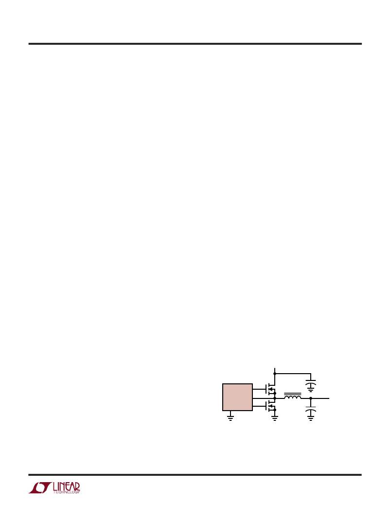
�Switching� Architecture�
�Each� half� of� the� LTC1702� is� designed� to� operate� as� a�
�synchronous� buck� converter� (Figure� 1).� Each� channel�
�includes� two� high� power� MOSFET� gate� drivers� to� control�
�external� N-channel� MOSFETs� QT� and� QB.� These� drivers�
�have� 0.5� ?� output� impedances� and� can� carry� well� over� an�
�V� IN�
�The� high� bandwidth� of� the� amplifier,� coupled� with� the� high�
�switching� frequency� and� the� low� values� of� the� external�
�+�
�C� IN�
�inductor� and� output� capacitor,� allow� very� high� loop� cross-�
�TG�
�QT�
�L� EXT�
�PGND�
�over� frequencies.� The� low� inductor� value� is� the� other� half�
�of� the� equation—with� a� typical� value� on� the� order� of� 1� μ� H,�
�LTC1702� SW�
�BG�
�QB�
�+�
�C� OUT�
�V� OUT�
�the� inductor� allows� very� fast� di/dt� slew� rates.� The� result� is�
�superior� transient� response� compared� with� conventional�
�solutions.�
�1702� F01�
�Figure� 1.� Synchronous� Buck� Architecture�
�1702fa�
�9�
�相关PDF资料 |
PDF描述 |
|---|---|
| RSC18DRTS | CONN EDGECARD 36POS DIP .100 SLD |
| H2AAT-10103-R4-ND | JUMPER-H1502TR/A2015R/H1502TR 3" |
| VE-25Z-EU-F1 | CONVERTER MOD DC/DC 2V 80W |
| SLP682M025C1P3 | CAP ALUM 6800UF 25V 20% SNAP |
| H2AAT-10103-N4-ND | JUMPER-H1502TR/A2015N/H1502TR 3" |
相关代理商/技术参数 |
参数描述 |
|---|---|
| LTC1702IGN#PBF | 功能描述:IC REG CTRLR BUCK PWM VM 24-SSOP RoHS:是 类别:集成电路 (IC) >> PMIC - 稳压器 - DC DC 切换控制器 系列:PolyPhase® 标准包装:4,500 系列:PowerWise® PWM 型:控制器 输出数:1 频率 - 最大:1MHz 占空比:95% 电源电压:2.8 V ~ 5.5 V 降压:是 升压:无 回扫:无 反相:无 倍增器:无 除法器:无 Cuk:无 隔离:无 工作温度:-40°C ~ 125°C 封装/外壳:6-WDFN 裸露焊盘 包装:带卷 (TR) 配用:LM1771EVAL-ND - BOARD EVALUATION LM1771 其它名称:LM1771SSDX |
| LTC1702IGN#TR | 功能描述:IC REG CTRLR BUCK PWM VM 24-SSOP RoHS:否 类别:集成电路 (IC) >> PMIC - 稳压器 - DC DC 切换控制器 系列:PolyPhase® 标准包装:4,500 系列:PowerWise® PWM 型:控制器 输出数:1 频率 - 最大:1MHz 占空比:95% 电源电压:2.8 V ~ 5.5 V 降压:是 升压:无 回扫:无 反相:无 倍增器:无 除法器:无 Cuk:无 隔离:无 工作温度:-40°C ~ 125°C 封装/外壳:6-WDFN 裸露焊盘 包装:带卷 (TR) 配用:LM1771EVAL-ND - BOARD EVALUATION LM1771 其它名称:LM1771SSDX |
| LTC1702IGN#TRPBF | 功能描述:IC REG CTRLR BUCK PWM VM 24-SSOP RoHS:是 类别:集成电路 (IC) >> PMIC - 稳压器 - DC DC 切换控制器 系列:PolyPhase® 标准包装:4,500 系列:PowerWise® PWM 型:控制器 输出数:1 频率 - 最大:1MHz 占空比:95% 电源电压:2.8 V ~ 5.5 V 降压:是 升压:无 回扫:无 反相:无 倍增器:无 除法器:无 Cuk:无 隔离:无 工作温度:-40°C ~ 125°C 封装/外壳:6-WDFN 裸露焊盘 包装:带卷 (TR) 配用:LM1771EVAL-ND - BOARD EVALUATION LM1771 其它名称:LM1771SSDX |
| LTC1703CG | 功能描述:IC REG SW DUAL SYNC VID 28SSOP RoHS:否 类别:集成电路 (IC) >> PMIC - 稳压器 - 专用型 系列:- 标准包装:43 系列:- 应用:控制器,Intel VR11 输入电压:5 V ~ 12 V 输出数:1 输出电压:0.5 V ~ 1.6 V 工作温度:-40°C ~ 85°C 安装类型:表面贴装 封装/外壳:48-VFQFN 裸露焊盘 供应商设备封装:48-QFN(7x7) 包装:管件 |
| LTC1703CG#PBF | 功能描述:IC REG SW DUAL SYNC VID 28SSOP RoHS:是 类别:集成电路 (IC) >> PMIC - 稳压器 - 专用型 系列:- 标准包装:2,000 系列:- 应用:控制器,DSP 输入电压:4.5 V ~ 25 V 输出数:2 输出电压:最低可调至 1.2V 工作温度:-40°C ~ 85°C 安装类型:表面贴装 封装/外壳:30-TFSOP(0.173",4.40mm 宽) 供应商设备封装:30-TSSOP 包装:带卷 (TR) |
发布紧急采购,3分钟左右您将得到回复。