- 您现在的位置:买卖IC网 > PDF目录10097 > LTC1744IFW (Linear Technology)IC ADC 14BIT 50MSPS 48-TSSOP PDF资料下载
参数资料
| 型号: | LTC1744IFW |
| 厂商: | Linear Technology |
| 文件页数: | 5/24页 |
| 文件大小: | 0K |
| 描述: | IC ADC 14BIT 50MSPS 48-TSSOP |
| 标准包装: | 39 |
| 位数: | 14 |
| 采样率(每秒): | 50M |
| 数据接口: | 并联 |
| 转换器数目: | 1 |
| 功率耗散(最大): | 1.5W |
| 电压电源: | 单电源 |
| 工作温度: | -40°C ~ 85°C |
| 安装类型: | 表面贴装 |
| 封装/外壳: | 48-TFSOP(0.240",6.10mm 宽) |
| 供应商设备封装: | 48-TSSOP |
| 包装: | 管件 |
| 输入数目和类型: | 2 个单端,双极;1 个差分,双极 |
13
LTC1744
1744f
APPLICATIO S I FOR ATIO
WU
U
given sampling capacitor size. The capacitors shown
attached to each input (CPARASITIC) are the summation of
all other capacitance associated with each input.
During the sample phase when ENC/ENC is low, the
transmission gate connects the analog inputs to the sam-
pling capacitors and they charge to and track the differen-
tial input voltage. When ENC/ENC transitions from low to
high the sampled input voltage is held on the sampling
capacitors. During the hold phase when ENC/ENC is high
the sampling capacitors are disconnected from the input
and the held voltage is passed to the ADC core for
processing. As ENC/ENC transitions from high to low the
inputs are reconnected to the sampling capacitors to
acquire a new sample. Since the sampling capacitors still
hold the previous sample, a charging glitch proportional to
the change in voltage between samples will be seen at this
time. If the change between the last sample and the new
sample is small the charging glitch seen at the input will be
small. If the input change is large, such as the change seen
with input frequencies near Nyquist, then a larger charging
glitch will be seen.
Common Mode Bias
The ADC sample-and-hold circuit requires differential
drive to achieve specified performance. Each input should
swing
±0.8V for the 3.2V range or ±0.5V for the 2V range,
around a common mode voltage of 2.5V. The VCM output
pin (Pin 2) may be used to provide the common mode bias
level. VCM can be tied directly to the center tap of a
transformer to set the DC input level or as a reference level
to an op amp differential driver circuit. The VCM pin must
be bypassed to ground close to the ADC with 4.7
F or
greater.
Input Drive Impedance
As with all high performance, high speed ADCs the dy-
namic performance of the LTC1744 can be influenced by
the input drive circuitry, particularly the second and third
harmonics. Source impedance and input reactance can
influence SFDR. At the falling edge of encode the sample-
and-hold circuit will connect the 7pF sampling capacitor to
the input pin and start the sampling period. The sampling
period ends when encode rises, holding the sampled input
on the sampling capacitor. Ideally the input circuitry
should be fast enough to fully charge the sampling capaci-
tor during the sampling period 1/(2FENCODE); however,
this is not always possible and the incomplete settling may
degrade the SFDR. The sampling glitch has been designed
to be as linear as possible to minimize the effects of
incomplete settling.
For the best performance, it is recomended to have a
source impedence of 100
or less for each input. The
source impedence should be matched for the differential
inputs. Poor matching will result in higher even order
harmonics, especially the second.
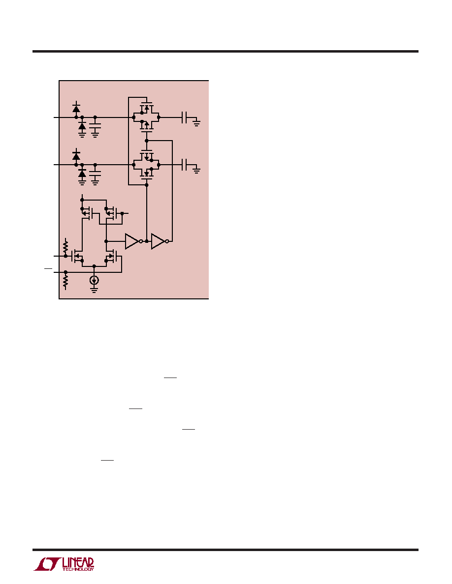
Figure 2. Equivalent Input Circuit
CSAMPLE
7pF
CPARASITIC
8pF
CPARASITIC
8pF
VDD
LTC1744
AIN
+
1744 F02
CSAMPLE
7pF
BIAS
VDD
5V
AIN
–
ENC
2V
6k
2V
6k
相关PDF资料 |
PDF描述 |
|---|---|
| VE-26B-MX-F1 | CONVERTER MOD DC/DC 95V 75W |
| VI-213-IU-F1 | CONVERTER MOD DC/DC 24V 200W |
| MS27484T14F97P | CONN PLUG 12POS STRAIGHT W/PINS |
| VE-263-MX-F3 | CONVERTER MOD DC/DC 24V 75W |
| VI-20Z-MY | CONVERTER MOD DC/DC 2V 20W |
相关代理商/技术参数 |
参数描述 |
|---|---|
| LTC1744IFW#PBF | 功能描述:IC ADC 14BIT 50MSPS 48-TSSOP RoHS:是 类别:集成电路 (IC) >> 数据采集 - 模数转换器 系列:- 标准包装:1 系列:- 位数:14 采样率(每秒):83k 数据接口:串行,并联 转换器数目:1 功率耗散(最大):95mW 电压电源:双 ± 工作温度:0°C ~ 70°C 安装类型:通孔 封装/外壳:28-DIP(0.600",15.24mm) 供应商设备封装:28-PDIP 包装:管件 输入数目和类型:1 个单端,双极 |
| LTC1744IFW#TR | 功能描述:IC ADC 14BIT 50MSPS 48-TSSOP RoHS:否 类别:集成电路 (IC) >> 数据采集 - 模数转换器 系列:- 标准包装:1 系列:- 位数:14 采样率(每秒):83k 数据接口:串行,并联 转换器数目:1 功率耗散(最大):95mW 电压电源:双 ± 工作温度:0°C ~ 70°C 安装类型:通孔 封装/外壳:28-DIP(0.600",15.24mm) 供应商设备封装:28-PDIP 包装:管件 输入数目和类型:1 个单端,双极 |
| LTC1744IFW#TRPBF | 功能描述:IC ADC 14BIT 50MSPS 48-TSSOP RoHS:是 类别:集成电路 (IC) >> 数据采集 - 模数转换器 系列:- 产品培训模块:Lead (SnPb) Finish for COTS Obsolescence Mitigation Program 标准包装:2,500 系列:- 位数:12 采样率(每秒):3M 数据接口:- 转换器数目:- 功率耗散(最大):- 电压电源:- 工作温度:- 安装类型:表面贴装 封装/外壳:SOT-23-6 供应商设备封装:SOT-23-6 包装:带卷 (TR) 输入数目和类型:- |
| LTC1745CFW | 功能描述:IC ADC 12BIT 25MSPS LN 48TSSOP RoHS:否 类别:集成电路 (IC) >> 数据采集 - 模数转换器 系列:- 标准包装:1,000 系列:- 位数:12 采样率(每秒):300k 数据接口:并联 转换器数目:1 功率耗散(最大):75mW 电压电源:单电源 工作温度:0°C ~ 70°C 安装类型:表面贴装 封装/外壳:24-SOIC(0.295",7.50mm 宽) 供应商设备封装:24-SOIC 包装:带卷 (TR) 输入数目和类型:1 个单端,单极;1 个单端,双极 |
| LTC1745CFW#PBF | 功能描述:IC ADC 12BIT 25MSPS LN 48TSSOP RoHS:是 类别:集成电路 (IC) >> 数据采集 - 模数转换器 系列:- 产品培训模块:Lead (SnPb) Finish for COTS Obsolescence Mitigation Program 标准包装:2,500 系列:- 位数:12 采样率(每秒):3M 数据接口:- 转换器数目:- 功率耗散(最大):- 电压电源:- 工作温度:- 安装类型:表面贴装 封装/外壳:SOT-23-6 供应商设备封装:SOT-23-6 包装:带卷 (TR) 输入数目和类型:- |
发布紧急采购,3分钟左右您将得到回复。