- 您现在的位置:买卖IC网 > PDF目录2004 > LTC1749IFW#PBF (Linear Technology)IC ADC 12BIT 80MSPS SMPL 48TSSOP PDF资料下载
参数资料
| 型号: | LTC1749IFW#PBF |
| 厂商: | Linear Technology |
| 文件页数: | 5/20页 |
| 文件大小: | 0K |
| 描述: | IC ADC 12BIT 80MSPS SMPL 48TSSOP |
| 标准包装: | 39 |
| 位数: | 12 |
| 采样率(每秒): | 80M |
| 数据接口: | 并联 |
| 转换器数目: | 1 |
| 功率耗散(最大): | 1.69W |
| 电压电源: | 单电源 |
| 工作温度: | -40°C ~ 85°C |
| 安装类型: | 表面贴装 |
| 封装/外壳: | 48-TFSOP(0.240",6.10mm 宽) |
| 供应商设备封装: | 48-TSSOP |
| 包装: | 管件 |
| 输入数目和类型: | 2 个单端,双极;1 个差分,双极 |
13
LTC1749
1749f
Input Drive Circuits
The LTC1749 requires differential drive for the analog
inputs. A balanced input drive will minimize even order
harmonics that are due to nonlinear behavior of the input
drive circuits and the S/H circuit.
The S/H circuit of the LTC1749 is a switched capacitor
circuit (Figure 2). The input drive circuitry will see a
sampling glitch at the start of the sampling period, when
ENC/ENC falls. Although designed to be linear as possible,
a small fraction of this glitch is nonlinear and can result in
additional observed distortion if the input drive circuitry is
too slow. For most practical circuits the glitch nonlinearity
is more than 100dB below the fundamental. The glitch will
decay during the sampling period with a time constant
determined by the input drive and S/H circuitry.
For fast settling and wide bandwidth, a low drive imped-
ance is required. The S/H bandwidth is partially deter-
mined by the source impedance. The full 500MHz
bandwidth is valid for source impedance (each input) less
than 30
. Higher source impedance can be used but full
amplitude distortion will be better with a source imped-
ance less than 100
.
Transformers
Transformers provide a simple method for converting a
single-ended signal to a differential signal; however, they
have poor performance characteristics at low and high input
frequencies. The lower –3dB corner of RF transformers can
range from tens of kHz to tens of MHz. Operation near this
corner results in poor 2nd order harmonic performance
due to nonlinear transformer core behavior. The upper
–3dB corner can vary from tens of MHz to several GHz.
Operation near the upper corner can result in poor 2nd order
performance due to poor balance on the secondary.
Transformers should be selected to have –3dB corners at
least one octave away from the desired operating fre-
quency. Transformers with larger cores usually have
better performance at lower frequency and perform better
when driving heavy loads.
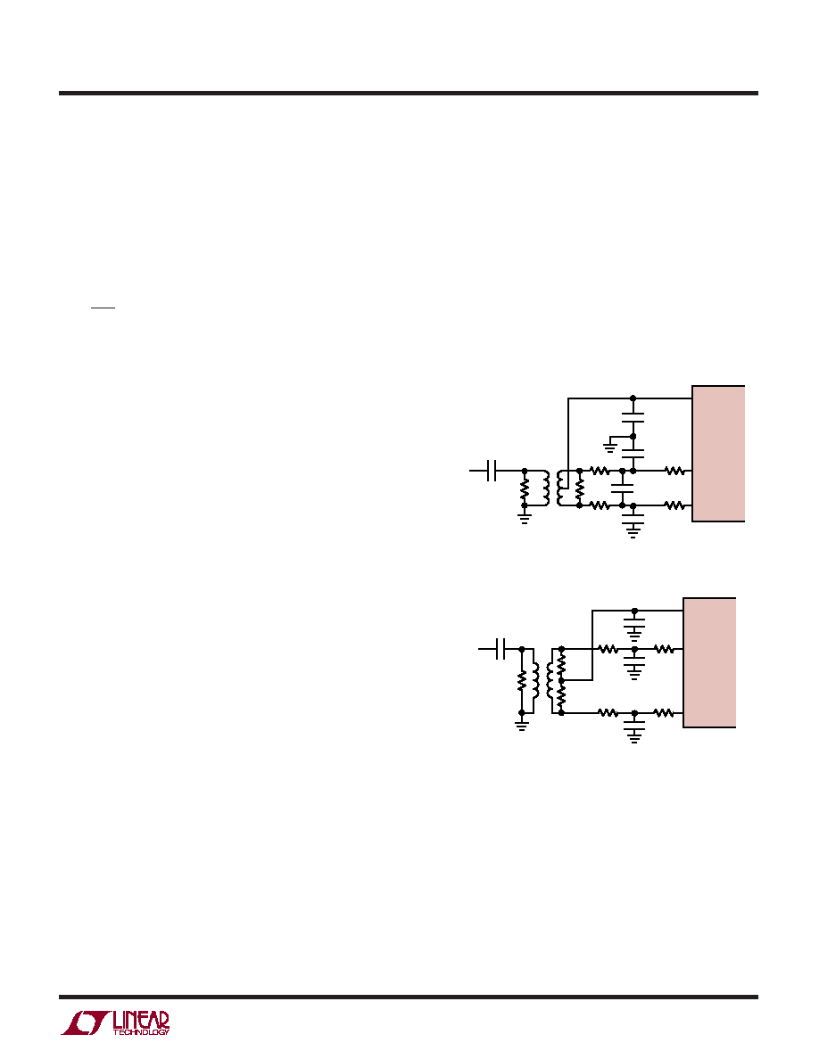
Figure 3a shows the LTC1749 being driven by an RF
transformer with a center tapped secondary. The second-
ary center tap is DC-biased with VCM, setting the ADC input
signal at its optimum DC level of 2V. In this example a 1:1
transformer is used; however, other transformer imped-
ance ratios may be substituted.
Figure 3b shows the use of a transformer without a center
tapped secondary. In this example the secondary is biased
with the addition of two resistors placed in series across
the secondary winding. The center tap of the secondary
resistors is connected to the ADC VCM output to set the DC
bias. This circuit is better suited for high input frequency
applications since center tapped transformers generally
have less bandwidth and poor balance at high frequencies
than noncenter tapped transformers.
APPLICATIO S I FOR ATIO
WU
UU
Figure 3a. Single-Ended to Differential
Conversion Using a Transformer
1:1
25
0.1
F
ANALOG
INPUT
100
100
12pF
1749 F03
4.7
F
25
25
25
LTC1749
VCM
AIN
+
AIN
–
1:4
10
0.1
F
ANALOG
INPUT
100
200
200
8.4pF
1749 F03b
10
25
25
8.4pF
4.7
F
LTC1749
VCM
AIN
+
AIN
–
Figure 3b. Using a Transformer
Without a Center Tapped Secondary
Active Drive Circuits
Active circuits, open loop or closed loop, can be used to
drive the ADC inputs. Closed-loop circuits such as op amps
have excellent DC and low frequency accuracy but have
poor high frequency performance. Figure 4 shows the dual
LT
1818 op amp used for single-ended to differential
signal conversion. Note that the two op amps do not have
the same noise gain, which can result in poor balance at
higher frequencies. The op amp configured in a gain of +1
相关PDF资料 |
PDF描述 |
|---|---|
| LTC1750IFW#PBF | IC ADC 14BIT 80MSPS SMPL 48TSSOP |
| LTC1799HS5#TRPBF | IC OSC SILICON 33MHZ TSOT23-5 |
| LTC1821ACGW | IC D/A CONV 16BIT PRECISE 36SSOP |
| LTC1851CFW | IC ADC 12BIT 1.25MSPS 48-TSSOP |
| LTC1853IFW#TRPBF | IC A/D CONV 8CH 12BIT 48-TSSOP |
相关代理商/技术参数 |
参数描述 |
|---|---|
| LTC1750CFW | 功能描述:IC ADC 14BIT 80MSPS SMPL 48TSSOP RoHS:否 类别:集成电路 (IC) >> 数据采集 - 模数转换器 系列:- 标准包装:1 系列:- 位数:14 采样率(每秒):83k 数据接口:串行,并联 转换器数目:1 功率耗散(最大):95mW 电压电源:双 ± 工作温度:0°C ~ 70°C 安装类型:通孔 封装/外壳:28-DIP(0.600",15.24mm) 供应商设备封装:28-PDIP 包装:管件 输入数目和类型:1 个单端,双极 |
| LTC1750CFW#PBF | 功能描述:IC ADC 14BIT 80MSPS SMPL 48TSSOP RoHS:是 类别:集成电路 (IC) >> 数据采集 - 模数转换器 系列:- 标准包装:1 系列:- 位数:14 采样率(每秒):83k 数据接口:串行,并联 转换器数目:1 功率耗散(最大):95mW 电压电源:双 ± 工作温度:0°C ~ 70°C 安装类型:通孔 封装/外壳:28-DIP(0.600",15.24mm) 供应商设备封装:28-PDIP 包装:管件 输入数目和类型:1 个单端,双极 |
| LTC1750CFW#TR | 功能描述:IC ADC 14BIT 80MSPS SMPL 48TSSOP RoHS:否 类别:集成电路 (IC) >> 数据采集 - 模数转换器 系列:- 标准包装:1 系列:- 位数:14 采样率(每秒):83k 数据接口:串行,并联 转换器数目:1 功率耗散(最大):95mW 电压电源:双 ± 工作温度:0°C ~ 70°C 安装类型:通孔 封装/外壳:28-DIP(0.600",15.24mm) 供应商设备封装:28-PDIP 包装:管件 输入数目和类型:1 个单端,双极 |
| LTC1750CFW#TRPBF | 功能描述:IC ADC 14BIT 80MSPS SMPL 48TSSOP RoHS:是 类别:集成电路 (IC) >> 数据采集 - 模数转换器 系列:- 标准包装:1 系列:- 位数:14 采样率(每秒):83k 数据接口:串行,并联 转换器数目:1 功率耗散(最大):95mW 电压电源:双 ± 工作温度:0°C ~ 70°C 安装类型:通孔 封装/外壳:28-DIP(0.600",15.24mm) 供应商设备封装:28-PDIP 包装:管件 输入数目和类型:1 个单端,双极 |
| LTC1750IFW | 功能描述:IC ADC 14BIT 80MSPS SMPL 48TSSOP RoHS:否 类别:集成电路 (IC) >> 数据采集 - 模数转换器 系列:- 标准包装:1 系列:- 位数:14 采样率(每秒):83k 数据接口:串行,并联 转换器数目:1 功率耗散(最大):95mW 电压电源:双 ± 工作温度:0°C ~ 70°C 安装类型:通孔 封装/外壳:28-DIP(0.600",15.24mm) 供应商设备封装:28-PDIP 包装:管件 输入数目和类型:1 个单端,双极 |
发布紧急采购,3分钟左右您将得到回复。