- 您现在的位置:买卖IC网 > PDF目录2004 > LTC1749IFW#PBF (Linear Technology)IC ADC 12BIT 80MSPS SMPL 48TSSOP PDF资料下载
参数资料
| 型号: | LTC1749IFW#PBF |
| 厂商: | Linear Technology |
| 文件页数: | 7/20页 |
| 文件大小: | 0K |
| 描述: | IC ADC 12BIT 80MSPS SMPL 48TSSOP |
| 标准包装: | 39 |
| 位数: | 12 |
| 采样率(每秒): | 80M |
| 数据接口: | 并联 |
| 转换器数目: | 1 |
| 功率耗散(最大): | 1.69W |
| 电压电源: | 单电源 |
| 工作温度: | -40°C ~ 85°C |
| 安装类型: | 表面贴装 |
| 封装/外壳: | 48-TFSOP(0.240",6.10mm 宽) |
| 供应商设备封装: | 48-TSSOP |
| 包装: | 管件 |
| 输入数目和类型: | 2 个单端,双极;1 个差分,双极 |
15
LTC1749
1749f
Input Range
The LTC1749 performance may be optimized by adjusting
the ADC’s input range to meet the requirements of the
application. For lower input frequency applications
(<40MHz), the highest input range of
±1.125V(2.25V)will
provide the best SNR while maintaining excellent SFDR.
For higher input frequencies (>80MHz), a lower input
range will provide better SFDR performance with a reduc-
tion in SNR.
The input range of the ADC is determined as
±VREF/APGA,
where VREF is the reference voltage (described in the
Reference Operation section) and APGA is the effective
APPLICATIO S I FOR ATIO
WU
UU
PGA gain. Table 1 shows the input range of the ADC versus
the state of the two pins, PGA and SENSE.
Driving the Encode Inputs
The noise performance of the LTC1749 can depend on the
encode signal quality as much as on the analog input. The
ENC/ENC inputs are intended to be driven differentially,
primarily for immunity from common mode noise sources.
Each input is biased through a 6k resistor to a 2V bias. The
bias resistors set the DC operating point for transformer
coupled drive circuits and can set the logic threshold for
single-ended drive circuits.
Any noise present on the encode signal will result in
additional aperture jitter that will be RMS summed with the
inherent ADC aperture jitter.
In applications where jitter is critical (high input frequen-
cies) take the following into consideration:
1. Differential drive should be used.
2. Use as large an amplitude as possible; if transformer
coupled use a higher turns ratio to increase the
amplitude.
3. If the ADC is clocked with a sinusoidal signal, filter the
encode signal to reduce wideband noise.
4. Balance the capacitance and series resistance at both
encode inputs so that any coupled noise will appear at
both inputs as common mode noise.
The encode inputs have a common mode range of 1.8V to
VDD. Each input may be driven from ground to VDD for
single-ended drive.
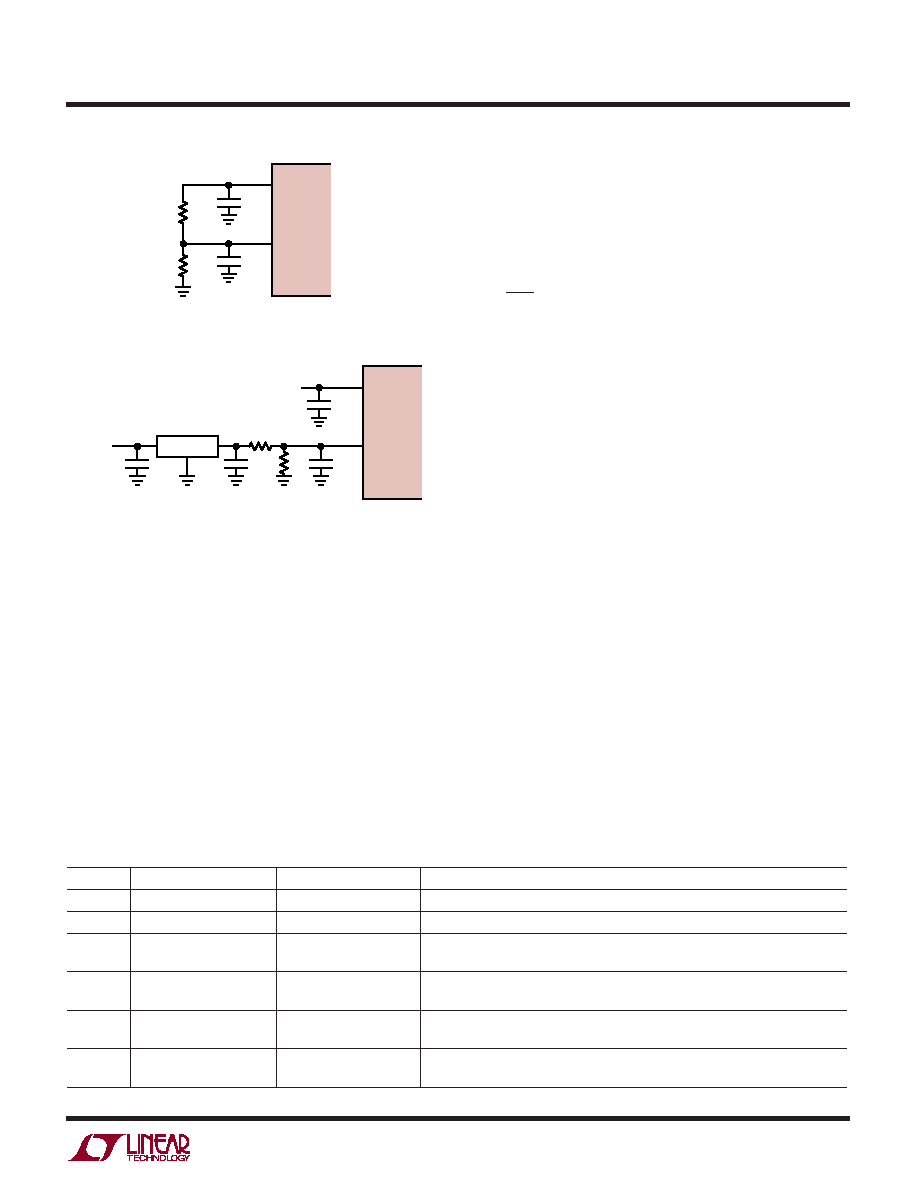
VCM
SENSE
2V
1V
4.7
F
10k
1
F
10k
1749 F06a
LTC1749
VCM
SENSE
2V
5V
2.5k
6
4
1, 2
4.7
F
1
F
1
F
10k
0.1
F
1749 F06b
LTC1749
LT1790-1.25
Figure 6a. 2V Range ADC
Figure 6b. 2V Range ADC with External Reference
Table 1
PGA
VSENSE
INPUT RANGE
COMMENTS
0= VDD
2.25VP-P Differential
Best Noise, SNR = 71.8dB. Good SFDR, >80dB Up to 100MHz
1= VDD
1.35VP-P Differential
Improved High Frequency Distortion. SNR = 70.5dB. SFDR > 80dB Up to 250MHz
0
= GND
1.4VP-P Differential
Reduced Internal Reference Mode with PGA = 0. Provides Similar Input Range as
VSENSE = VDD and PGA = 0 But with Worse Noise. SNR = 70.3dB
1
= GND
0.84VP-P Differential
Smallest Possible Input Span. Useful for Improved Distortion at Very High
Frequencies, But with Reduced Noise Performance. SNR = 69dB
0
0.7V < VSENSE < 1.125V
2
× VSENSE Differential
Adjustable Input Range with Better Noise Performance. SNR = 71.8dB with
VSENSE = 1.125V, SNR = 70.3dB with VSENSE = 0.7V
1
0.7V < VSENSE < 1.125V
1.2
× VSENSE Differential
Adjustable Input Range with Better High Frequency Distortion. SNR = 70.5dB with
VSENSE = 1.125V, SNR = 69dB with VSENSE = 0.7V
相关PDF资料 |
PDF描述 |
|---|---|
| LTC1750IFW#PBF | IC ADC 14BIT 80MSPS SMPL 48TSSOP |
| LTC1799HS5#TRPBF | IC OSC SILICON 33MHZ TSOT23-5 |
| LTC1821ACGW | IC D/A CONV 16BIT PRECISE 36SSOP |
| LTC1851CFW | IC ADC 12BIT 1.25MSPS 48-TSSOP |
| LTC1853IFW#TRPBF | IC A/D CONV 8CH 12BIT 48-TSSOP |
相关代理商/技术参数 |
参数描述 |
|---|---|
| LTC1750CFW | 功能描述:IC ADC 14BIT 80MSPS SMPL 48TSSOP RoHS:否 类别:集成电路 (IC) >> 数据采集 - 模数转换器 系列:- 标准包装:1 系列:- 位数:14 采样率(每秒):83k 数据接口:串行,并联 转换器数目:1 功率耗散(最大):95mW 电压电源:双 ± 工作温度:0°C ~ 70°C 安装类型:通孔 封装/外壳:28-DIP(0.600",15.24mm) 供应商设备封装:28-PDIP 包装:管件 输入数目和类型:1 个单端,双极 |
| LTC1750CFW#PBF | 功能描述:IC ADC 14BIT 80MSPS SMPL 48TSSOP RoHS:是 类别:集成电路 (IC) >> 数据采集 - 模数转换器 系列:- 标准包装:1 系列:- 位数:14 采样率(每秒):83k 数据接口:串行,并联 转换器数目:1 功率耗散(最大):95mW 电压电源:双 ± 工作温度:0°C ~ 70°C 安装类型:通孔 封装/外壳:28-DIP(0.600",15.24mm) 供应商设备封装:28-PDIP 包装:管件 输入数目和类型:1 个单端,双极 |
| LTC1750CFW#TR | 功能描述:IC ADC 14BIT 80MSPS SMPL 48TSSOP RoHS:否 类别:集成电路 (IC) >> 数据采集 - 模数转换器 系列:- 标准包装:1 系列:- 位数:14 采样率(每秒):83k 数据接口:串行,并联 转换器数目:1 功率耗散(最大):95mW 电压电源:双 ± 工作温度:0°C ~ 70°C 安装类型:通孔 封装/外壳:28-DIP(0.600",15.24mm) 供应商设备封装:28-PDIP 包装:管件 输入数目和类型:1 个单端,双极 |
| LTC1750CFW#TRPBF | 功能描述:IC ADC 14BIT 80MSPS SMPL 48TSSOP RoHS:是 类别:集成电路 (IC) >> 数据采集 - 模数转换器 系列:- 标准包装:1 系列:- 位数:14 采样率(每秒):83k 数据接口:串行,并联 转换器数目:1 功率耗散(最大):95mW 电压电源:双 ± 工作温度:0°C ~ 70°C 安装类型:通孔 封装/外壳:28-DIP(0.600",15.24mm) 供应商设备封装:28-PDIP 包装:管件 输入数目和类型:1 个单端,双极 |
| LTC1750IFW | 功能描述:IC ADC 14BIT 80MSPS SMPL 48TSSOP RoHS:否 类别:集成电路 (IC) >> 数据采集 - 模数转换器 系列:- 标准包装:1 系列:- 位数:14 采样率(每秒):83k 数据接口:串行,并联 转换器数目:1 功率耗散(最大):95mW 电压电源:双 ± 工作温度:0°C ~ 70°C 安装类型:通孔 封装/外壳:28-DIP(0.600",15.24mm) 供应商设备封装:28-PDIP 包装:管件 输入数目和类型:1 个单端,双极 |
发布紧急采购,3分钟左右您将得到回复。