- 您现在的位置:买卖IC网 > PDF目录2004 > LTC1749IFW#PBF (Linear Technology)IC ADC 12BIT 80MSPS SMPL 48TSSOP PDF资料下载
参数资料
| 型号: | LTC1749IFW#PBF |
| 厂商: | Linear Technology |
| 文件页数: | 6/20页 |
| 文件大小: | 0K |
| 描述: | IC ADC 12BIT 80MSPS SMPL 48TSSOP |
| 标准包装: | 39 |
| 位数: | 12 |
| 采样率(每秒): | 80M |
| 数据接口: | 并联 |
| 转换器数目: | 1 |
| 功率耗散(最大): | 1.69W |
| 电压电源: | 单电源 |
| 工作温度: | -40°C ~ 85°C |
| 安装类型: | 表面贴装 |
| 封装/外壳: | 48-TFSOP(0.240",6.10mm 宽) |
| 供应商设备封装: | 48-TSSOP |
| 包装: | 管件 |
| 输入数目和类型: | 2 个单端,双极;1 个差分,双极 |
14
LTC1749
1749f
can be configured in a noise gain of +2 with the addition of
two equal valued resistors between the output and invert-
ing input and between the two inputs. This however will raise
the noise contributed by the op amps.
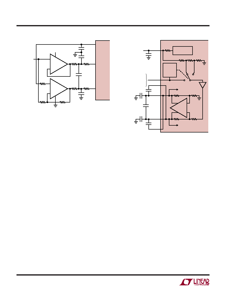
Reference Operation
Figure 5 shows the LTC1749 equivalent reference circuitry
consisting of a 2V bandgap reference, a 3-to-1 switch, a
switch control circuit and a difference amplifier.
The 2V bandgap reference serves two functions. First, it is
assessable at the VCM pin to provide a DC bias point for
setting the common mode voltage of any external input
circuitry. Second, it is used to derive internal reference
levels that may be used to set the input range of the ADC.
An external bypass capacitor is required for the 2V refer-
ence output at the VCM pin. This provides a high frequency
low impedance path to ground for internal and external
circuitry. This is also the compensation capacitor for the
reference, which will not be stable without this capacitor.
To achieve the optimal input range for an application, the
internal reference voltage (VREF) is flexible. The reference
switch shown in Figure 5 connects VREF to one of two
internally derived reference voltages, or to an externally
derived reference voltage. The internally derived refer-
ences are selected by strapping the SENSE pin to GND for
0.7V, or to VDD for 1.125V. When 0.7V > VSENSE > 1.125V,
VSENSE is directly connected to VREF. Because of the dual
nature of the SENSE pin, driving it with a logic device is not
recommended.
Reference voltages between 0.7V and 1.125V may be
programmed with two external resistors as shown in
Figure 6a. An external reference may be used by applying
its output directly or through a resistor divider to the
SENSE pin (Figure 6b). When the SENSE pin is driven with
an externally derived reference voltage, it should be by-
passed to ground as close to the device as possible with
a 1
F ceramic capacitor.
A difference amplifier generates the high and low refer-
ences for the ADC. High speed switching circuits are
connected to these outputs and they must be externally
bypassed. Each output has two pins: REFHA and REFHB
for the high reference and REFLA and REFLB for the low
reference. The doubled output pins are needed to reduce
package inductance. Bypass capacitors must be con-
nected as shown in Figure 5.
APPLICATIO S I FOR ATIO
WU
UU
VCM
REFHA
REFLB
SENSE
TIE TO VDD FOR VREF = 1.125;
TIE TO GND FOR VREF = 0.7V;
VREF = VSENSE FOR
0.7V < VSENSE < 1.125V
2V
REFLA
REFHB
4.7
F
4.7
F
INTERNAL ADC
HIGH REFERENCE
BUFFER
VREF
0.1
F
1749 F05
LTC1749
4
DIFF AMP
1
F
1
F
0.1
F
INTERNAL ADC
LOW REFERENCE
2V BANDGAP
REFERENCE
1.125V 0.7V
RANGE
DETECT
AND
CONTROL
Figure 5. Equivalent Reference Circuit
Figure 4. Differential Drive with Op Amps
25
5V
SINGLE-ENDED
INPUT
2V
±1/2
RANGE
VCM
AIN
+
AIN
–
12pF
1749 F04
4.7
F
25
100
500
500
25
25
LTC1749
–
+
1/2 LT1818
–
+
1/2 LT1818
相关PDF资料 |
PDF描述 |
|---|---|
| LTC1750IFW#PBF | IC ADC 14BIT 80MSPS SMPL 48TSSOP |
| LTC1799HS5#TRPBF | IC OSC SILICON 33MHZ TSOT23-5 |
| LTC1821ACGW | IC D/A CONV 16BIT PRECISE 36SSOP |
| LTC1851CFW | IC ADC 12BIT 1.25MSPS 48-TSSOP |
| LTC1853IFW#TRPBF | IC A/D CONV 8CH 12BIT 48-TSSOP |
相关代理商/技术参数 |
参数描述 |
|---|---|
| LTC1750CFW | 功能描述:IC ADC 14BIT 80MSPS SMPL 48TSSOP RoHS:否 类别:集成电路 (IC) >> 数据采集 - 模数转换器 系列:- 标准包装:1 系列:- 位数:14 采样率(每秒):83k 数据接口:串行,并联 转换器数目:1 功率耗散(最大):95mW 电压电源:双 ± 工作温度:0°C ~ 70°C 安装类型:通孔 封装/外壳:28-DIP(0.600",15.24mm) 供应商设备封装:28-PDIP 包装:管件 输入数目和类型:1 个单端,双极 |
| LTC1750CFW#PBF | 功能描述:IC ADC 14BIT 80MSPS SMPL 48TSSOP RoHS:是 类别:集成电路 (IC) >> 数据采集 - 模数转换器 系列:- 标准包装:1 系列:- 位数:14 采样率(每秒):83k 数据接口:串行,并联 转换器数目:1 功率耗散(最大):95mW 电压电源:双 ± 工作温度:0°C ~ 70°C 安装类型:通孔 封装/外壳:28-DIP(0.600",15.24mm) 供应商设备封装:28-PDIP 包装:管件 输入数目和类型:1 个单端,双极 |
| LTC1750CFW#TR | 功能描述:IC ADC 14BIT 80MSPS SMPL 48TSSOP RoHS:否 类别:集成电路 (IC) >> 数据采集 - 模数转换器 系列:- 标准包装:1 系列:- 位数:14 采样率(每秒):83k 数据接口:串行,并联 转换器数目:1 功率耗散(最大):95mW 电压电源:双 ± 工作温度:0°C ~ 70°C 安装类型:通孔 封装/外壳:28-DIP(0.600",15.24mm) 供应商设备封装:28-PDIP 包装:管件 输入数目和类型:1 个单端,双极 |
| LTC1750CFW#TRPBF | 功能描述:IC ADC 14BIT 80MSPS SMPL 48TSSOP RoHS:是 类别:集成电路 (IC) >> 数据采集 - 模数转换器 系列:- 标准包装:1 系列:- 位数:14 采样率(每秒):83k 数据接口:串行,并联 转换器数目:1 功率耗散(最大):95mW 电压电源:双 ± 工作温度:0°C ~ 70°C 安装类型:通孔 封装/外壳:28-DIP(0.600",15.24mm) 供应商设备封装:28-PDIP 包装:管件 输入数目和类型:1 个单端,双极 |
| LTC1750IFW | 功能描述:IC ADC 14BIT 80MSPS SMPL 48TSSOP RoHS:否 类别:集成电路 (IC) >> 数据采集 - 模数转换器 系列:- 标准包装:1 系列:- 位数:14 采样率(每秒):83k 数据接口:串行,并联 转换器数目:1 功率耗散(最大):95mW 电压电源:双 ± 工作温度:0°C ~ 70°C 安装类型:通孔 封装/外壳:28-DIP(0.600",15.24mm) 供应商设备封装:28-PDIP 包装:管件 输入数目和类型:1 个单端,双极 |
发布紧急采购,3分钟左右您将得到回复。